
Data Sheet


VS1000 Datasheet
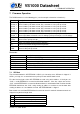
6 VS1000 FUNCTIONAL BLOCKS
6 VS1000 Functional Blocks
Reference
Regulator
Regulator
Regulator
Common
Voltage
Driver
Voltage
Monitor
Stereo
Earphone
Driver
Stereo
DAC
AVDD1
AVDD2
AVDD3
Serial
Data/
Control
Interface
UART
Clock
NAND
Flash
Interface/
General IO
<1.6V
USB
X RAM
X ROM
Y RAM
Y ROM
I RAM
I ROM
VSDSP4
processor
USBP
USPN
XCS/GPIO1[0]
SCLK/GPIO1[1]
SI/GPIO1[2]
SO/GPIO1[3]
RX/GPIO1[5]
TX/GPIO1[4]
XTALO
XTALI
Data/
GPIO0[0...7]
Control/
GPIO0[8...14]
XRESETTEST
IOVDD
AVDD
CVDD
IOVDD1
IOVDD2
PWRBTN
VHIGHRCAPCBUFRIGHTLEFT
reset
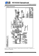
Figure 6: VS1000 block diagram.
6.1 Regulator Section
The VHIGH pin in the regulator section is used as a common main power supply for voltage
regulation. This input is connected to three internal regulators, which are activated when the
PWRBTN pin is set high (at least 2.3 V) for 1 to 10 milliseconds, so that AVDD starts to rise
and reaches about 1.5 V. After the PWRBTN has given this initial start current, the regulators
reach their default voltages even if the PWRBTN is released. VHIGH must be sufficiently (about
0.3 V) above the highest regulated power (normally AVDD) so that regulation can be properly
performed.
The PWRBTN state can also be read by software, so it can be used as one of the user interface
buttons.
A power-on reset monitors the core voltage and asserts reset if CVDD drops below the CMON
level. It is also possible to force a reset by keeping PWRBTN pressed for longer than approx-
imately 5.6 seconds. A watchdog counter and the XRESET pin can also generate a reset for
the device.
Resets do not cause the regulators to shut down, but they restore the default regulator voltages.
After boot the firmware and user software can change the voltages.
Return to power-off is possible only with active software control (VSDSP writes the regulator
Version: 1.5, 2016-06-09 16