
Data Sheet

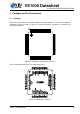


VS1000 Datasheet
3 CHARACTERISTICS & SPECIFICATIONS
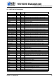
3.10 Analog Characteristics of USB
Parameter Min Max Unit
Drive low level, 2.32 mA load 0.065 0.102 V
Drive low level, 6.1×AVDD mA load 0.171×AVDD 0.270×AVDD V
Drive low level, 10.71×AVDD mA load 0.300×AVDD AVDD V
Drive high level, -2.32 mA load AVDD-0.165 AVDD-0.065 V
Drive high level, -6.1×AVDD mA load 0.650×AVDD 0.829×AVDD V
Drive high level, -10.71×AVDD mA load 0 0.700×AVDD V
USBP level, with 15 kΩ pull-down 2.7 0.943×AVDD V
High-Level input voltage (single-ended) 0.7×AVDD AVDD+0.3 V
Low-Level input voltage (single-ended) -0.2 0.3×AVDD V
Differential input common voltage, AVDD≥3.3V 0.8 2.5 V
Differential input signal level, AVDD≥3.3V 200 mV
Input leakage current -2.0 2.0 µA
3.11 Power Consumption
Parameter Symbol Min Typ Max Unit
Current Consumption of AVDD, no signal 3.4 mA
Current Consumption of AVDD, sine test, CBUF + 30Ω load 33 55 mA
Current Consumption of CVDD, sine test 3.0× clock 13 25 mA
Current Consumption of USB suspend mode
1
650 µA
Current Consumption, Reset @ 25
◦
C 24 48 µA
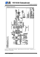
Example application (see Section 5) IOVDD=3.3V AVDD=2.8V CVDD=2.5V
Total Power, play mode, CBUF + 30Ω load 120 mW
Example application (see Section 5) IOVDD=2.7V AVDD=2.6V CVDD=2.2V
Total Power, pause mode 10 mW
Total Power, play mode, CBUF + 30Ω load 80 mW
1
Requires user code support
3.12 Digital Characteristics
Parameter Sym Min Typ Max Unit
High-Level Input Voltage 0.7×IOVDD IOVDD+0.3 V
Low-Level Input Voltage -0.2 0.3×IOVDD V
High-Level Output Voltage, -1.0 mA load
1
0.7×IOVDD V
Low-Level Output Voltage, 1.0 mA load
1
0.3×IOVDD V
XTALO high-level output voltage, -0.1 mA load 0.7×IOVDD V
XTALO low-level output voltage, 0.1 mA load 0.3×IOVDD V
Input leakage current -1.0 1.0 µA
Rise time of all output pins, load = 30 pF
1
50 ns
1
Pins GPIO0_[14:0], GPIO1_[5:0].
Version: 1.5, 2016-06-09 11