
User Manual


MCP2551
DS21667F-page 4 © 2010 Microchip Technology Inc.
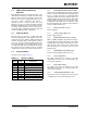
TABLE 1-1: MODES OF OPERATION
TABLE 1-2: TRANSCEIVER TRUTH TABLE
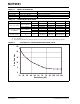
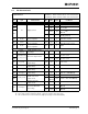
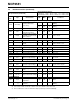
FIGURE 1-1: SLEW RATE VS. SLOPE-CONTROL RESISTANCE VALUE
Mode Current at R
s
Pin Resulting Voltage at RS Pin
Standby -I
RS < 10 µA VRS > 0.75 VDD
Slope-Control 10 µA < -IRS < 200 µA 0.4 VDD < VRS < 0.6 VDD
High-Speed -IRS < 610 µA 0 < VRS < 0.3VDD
VDD VRS TXD CANH CANL Bus State
(1)
RXD
(1)
4.5V ≤ VDD ≤ 5.5V
V
RS < 0.75 VDD
0 HIGH LOW Dominant 0
1 or floating Not Driven Not Driven Recessive 1
V
RS > 0.75 VDD X Not Driven Not Driven Recessive 1
VPOR
< VDD < 4.5V
(See Note 3)
V
RS < 0.75 VDD
0 HIGH LOW Dominant 0
1 or floating Not Driven Not Driven Recessive 1
V
RS > 0.75 VDD X Not Driven Not Driven Recessive 1
0 < VDD < VPOR XX
Not Driven/
No Load
Not Driven/
No Load
High Impedance X
Note 1: If another bus node is transmitting a Dominant bit on the CAN bus, then RXD is a logic ‘0’.
2: X = “don’t care”.
3: Device drivers will function, although outputs are not ensured to meet the ISO-11898 specification.
0
5
10
15
20
25
10 20 30 40 49 60 70 76 90 100 110 120
Resistance (k)
Slew Rate V/μs