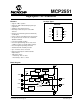
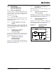
MCP2551 High-Speed CAN Transceiver Package Types • Supports 1 Mb/s operation • Implements ISO-11898 standard physical layer requirements • Suitable for 12V and 24V systems • Externally-controlled slope for reduced RFI emissions • Detection of ground fault (permanent Dominant) on TXD input • Power-on Reset and voltage brown-out protection • An unpowered node or brown-out event will not disturb the CAN bus • Low current standby operation • Protection against damage due to short-circuit conditions (positive o
MCP2551 NOTES: DS21667F-page 2 © 2010 Microchip Technology Inc.
MCP2551 1.0 DEVICE OVERVIEW 1.4 Operating Modes The MCP2551 is a high-speed CAN, fault-tolerant device that serves as the interface between a CAN protocol controller and the physical bus. The MCP2551 device provides differential transmit and receive capability for the CAN protocol controller, and is fully compatible with the ISO-11898 standard, including 24V requirements. It will operate at speeds of up to 1 Mb/s.
MCP2551 TABLE 1-1: MODES OF OPERATION Mode Current at Rs Pin Standby Slope-Control High-Speed Resulting Voltage at RS Pin -IRS < 10 µA 10 µA < -IRS < 200 µA -IRS < 610 µA TABLE 1-2: VRS > 0.75 VDD 0.4 VDD < VRS < 0.6 VDD 0 < VRS < 0.3VDD TRANSCEIVER TRUTH TABLE VDD VRS TXD CANH Bus State( 1) CANL HIGH LOW Dominant Not Driven Not Driven Recessive Not Driven Not Driven Recessive VRS > 0.75 VDD HIGH LOW Dominant VRS < 0.75 VDD VPOR < VDD < 4.
MCP2551 1.5 TXD Permanent Dominant Detection If the MCP2551 detects an extended Low state on the TXD input, it will disable the CANH and CANL output drivers in order to prevent the corruption of data on the CAN bus. The drivers are disabled if TXD is Low for more than 1.25 ms (minimum). This implies a maximum bit time of 62.5 µs (16 kb/s bus rate), allowing up to 20 consecutive transmitted Dominant bits during a multiple bit error and error frame scenario.
MCP2551 NOTES: DS21667F-page 6 © 2010 Microchip Technology Inc.
MCP2551 2.0 ELECTRICAL CHARACTERISTICS 2.1 Terms and Definitions A number of terms are defined in ISO-11898 that are used to describe the electrical characteristics of a CAN transceiver device. These terms and definitions are summarized in this section. 2.1.1 BUS VOLTAGE VCANL and VCANH denote the voltages of the bus line wires CANL and CANH relative to ground of each individual CAN node. 2.1.
MCP2551 Absolute Maximum Ratings† VDD .............................................................................................................................................................................7.0V DC Voltage at TXD, RXD, VREF and VS ............................................................................................ -0.3V to VDD + 0.3V DC Voltage at CANH, CANL (Note 1) ..........................................................................................................
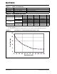
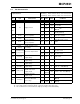
MCP2551 2.2 DC Characteristics Electrical Characteristics: Industrial (I): TAMB = -40°C to +85°C VDD = 4.5V to 5.5V Extended (E): TAMB = -40°C to +125°C VDD = 4.5V to 5.5V DC Specifications Param No. Sym Characteristic Min Max Units Conditions D1 — 75 mA Dominant; VTXD = 0.
MCP2551 2.2 DC Characteristics (Continued) Electrical Characteristics: Industrial (I): TAMB = -40°C to +85°C VDD = 4.5V to 5.5V Extended (E): TAMB = -40°C to +125°C VDD = 4.5V to 5.5V DC Specifications (Continued) Param No. Sym Characteristic Min Max Units Conditions Bus Line (CANH; CANL) Receiver: [TXD = 2V; pins 6 and 7 externally driven] D18 D19 VDIFF(d)(i) VDIFF(h)(i) D20 RIN D21 RIN(d) Dominant differential input voltage Differential input hysteresis 0.9 5.
MCP2551 FIGURE 2-1: TEST CIRCUIT FOR ELECTRICAL CHARACTERISTICS 0.1µF VDD CANH TXD VREF CAN Transceiver 60 Ω 100 pF RXD CANL 30 pF RS GND Rext Note: FIGURE 2-2: RS may be connected to VDD or GND via a load resistor depending on desired operating mode as described in Section 1.7.3 “Supply Voltage (VDD)”.
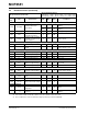
MCP2551 2.3 AC Characteristics Electrical Characteristics: Industrial (I): TAMB = -40°C to +85°C VDD = 4.5V to 5.5V Extended (E): TAMB = -40°C to +125°C VDD = 4.5V to 5.5V AC Specifications Param No. Sym 1 tBIT 2 fBIT 3 TtxL2bus(d) 4 5 6 TtxH2bus(r) TtxL2rx(d) TtxH2rx(r) Characteristic Min Max Units Bit time 1 62.
MCP2551 2.4 Timing Diagrams and Specifications FIGURE 2-4: TIMING DIAGRAM FOR AC CHARACTERISTICS VDD TXD (transmit data input voltage) 0V VDIFF (CANH, CANL differential voltage) RXD (receive data output voltage) 0.5V 0.9V 0.7 VDD 0.3 VDD 3 4 5 6 FIGURE 2-5: TIMING DIAGRAM FOR WAKE-UP FROM STANDBY VRS Slope resistor input voltage VDD 0.6 VDD 0V VRXD Receive data output voltage 0.3 VDD 10 VTXD = 0.8V FIGURE 2-6: TIMING DIAGRAM FOR BUS DOMINANT TO RXD LOW (STANDBY MODE) 1.
MCP2551 NOTES: DS21667F-page 14 © 2010 Microchip Technology Inc.
MCP2551 3.0 PACKAGING INFORMATION 3.1 Package Marking Information 8-Lead PDIP (300 mil) XXXXXXXX XXXXXNNN YYWW 8-Lead SOIC (150 mil) XXXXXXXX XXXXYYWW NNN Legend: XX...
MCP2551 3 & ' !& " & 4 # * !( ! ! & 4 % & & # & && 255*** ' '5 4 N NOTE 1 E1 1 3 2 D E A2 A L A1 c e eB b1 b 6 &! ' ! 9 ' &! 7"') % ! 7,8. 7 7 & ; < & & 7: 1 , = = - 1 ! & & = = .
MCP2551 ! "" #$ %& ! ' 3 & ' !& " & 4 # * !( ! ! & 4 % & & # & && 255*** ' '5 4 D e N E E1 NOTE 1 1 2 3 α h b h A2 A c φ L A1 L1 6 &! ' ! 9 ' &! 7"') % ! β 99 . . 7 7 7: ; < & : 8 & = = = = = # # 4 4 !! & # %% + 1 , : > #& . # # 4 > #& .
MCP2551 ! "" #$ %& ! ' 3 & ' !& " & 4 # * !( ! ! & 4 % & & # & && 255*** ' '5 4 DS21667F-page 18 © 2010 Microchip Technology Inc.
MCP2551 APPENDIX A: REVISION HISTORY Revision F (July 2010) The following is the list of modifications: 1. Updates to the packaging diagrams. Revision E (January 2007) The following is the list of modifications: 1. Updates to the packaging diagrams. Revision D (October 2003) The following is the list of modifications: 1. Undocumented changes. Revision C (November 2002) The following is the list of modifications: 1. Undocumented changes.
MCP2551 NOTES: DS21667F-page 20 © 2010 Microchip Technology Inc.
MCP2551 PRODUCT IDENTIFICATION SYSTEM To order or obtain information, e.g., on pricing or delivery, refer to the factory or the listed sales office. PART NO. -X /XX XXX Device Temperature Range Package Pattern Examples: a) b) Device: MCP2551: High-Speed CAN Transceiver MCP2551T: High-Speed CAN Transceiver (Tape and Reel) c) d) Temperature Range: I E Package: P SN = = -40°C to +85°C -40°C to +125°C = = © 2010 Microchip Technology Inc.
MCP2551 NOTES: DS21667F-page 22 © 2010 Microchip Technology Inc.
Note the following details of the code protection feature on Microchip devices: • Microchip products meet the specification contained in their particular Microchip Data Sheet. • Microchip believes that its family of products is one of the most secure families of its kind on the market today, when used in the intended manner and under normal conditions. • There are dishonest and possibly illegal methods used to breach the code protection feature.
WORLDWIDE SALES AND SERVICE AMERICAS ASIA/PACIFIC ASIA/PACIFIC EUROPE Corporate Office 2355 West Chandler Blvd. Chandler, AZ 85224-6199 Tel: 480-792-7200 Fax: 480-792-7277 Technical Support: http://support.microchip.com Web Address: www.microchip.