
MCP9700 Specifications
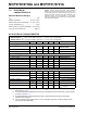
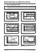
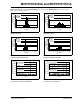
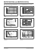
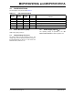
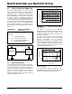
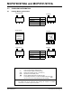
Table Of Contents
- 1.0 Electrical Characteristics
- 2.0 Typical Performance Curves
- FIGURE 2-1: Accuracy vs. Ambient Temperature (MCP9700A/9701A).
- FIGURE 2-2: Accuracy vs. Ambient Temperature, with VDD.
- FIGURE 2-3: Supply Current vs. Temperature.
- FIGURE 2-4: Accuracy vs. Ambient Temperature (MCP9700/9701).
- FIGURE 2-5: Changes in Accuracy vs. Ambient Temperature (Due to Load).
- FIGURE 2-6: Load Regulation vs. Ambient Temperature.
- FIGURE 2-7: Output Voltage at 0˚C (MCP9700/9700A).
- FIGURE 2-8: Occurrences vs. Temperature Coefficient (MCP9700/9700A).
- FIGURE 2-9: Power Supply Rejection (D˚C/DVDD) vs. Ambient Temperature.
- FIGURE 2-10: Output Voltage at 0˚C (MCP9701/9701A).
- FIGURE 2-11: Occurrences vs. Temperature Coefficient (MCP9701/9701A).
- FIGURE 2-12: Power Supply Rejection (D˚C/DVDD) vs. Temperature.
- FIGURE 2-13: Output Voltage vs. Power Supply.
- FIGURE 2-14: Output vs. Settling Time to step VDD.
- FIGURE 2-15: Thermal Response (Air to Fluid Bath).
- FIGURE 2-16: Output Voltage vs. Ambient Temperature.
- FIGURE 2-17: Output vs. Settling Time to Ramp VDD.
- FIGURE 2-18: Output Impedance vs. Frequency.
- 3.0 Pin Descriptions
- 4.0 Applications Information
- 5.0 Packaging Information

© 2007 Microchip Technology Inc. DS21942D-page 7
MCP9700/9700A and MCP9701/9701A
3.0 PIN DESCRIPTIONS
The descriptions of the pins are listed Ta ble 3- 1 .
TABLE 3-1: PIN FUNCTION TABLE
3.1 Power Ground Pin (GND)
GND is the system ground pin.
3.2 Output Voltage Pin (V
OUT
)
The sensor output can be measured at V
OUT
. The
voltage range over the operating temperature range for
the MCP9700/9700A is 100 mV to 1.75V and for the
MCP9701/9701A, 200 mV to 3V .
3.3 Power Supply Input (V
DD
)
The operating voltage as specified in the “DC
Electrical Characteristics” table is applied to V
DD
.
Pin No.
SC-70
Pin No.
SOT-23
Pin No.
TO-92
Symbol Function
1 — — NC No Connect
2 3 3 GND Power Ground Pin
322V
OUT
Output Voltage Pin
411V
DD
Power Supply Input
5 — — NC No Connect