
MCP9700 Specifications
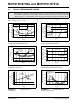
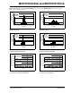
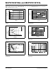
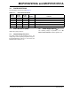
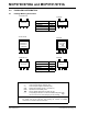
Table Of Contents
- 1.0 Electrical Characteristics
- 2.0 Typical Performance Curves
- FIGURE 2-1: Accuracy vs. Ambient Temperature (MCP9700A/9701A).
- FIGURE 2-2: Accuracy vs. Ambient Temperature, with VDD.
- FIGURE 2-3: Supply Current vs. Temperature.
- FIGURE 2-4: Accuracy vs. Ambient Temperature (MCP9700/9701).
- FIGURE 2-5: Changes in Accuracy vs. Ambient Temperature (Due to Load).
- FIGURE 2-6: Load Regulation vs. Ambient Temperature.
- FIGURE 2-7: Output Voltage at 0˚C (MCP9700/9700A).
- FIGURE 2-8: Occurrences vs. Temperature Coefficient (MCP9700/9700A).
- FIGURE 2-9: Power Supply Rejection (D˚C/DVDD) vs. Ambient Temperature.
- FIGURE 2-10: Output Voltage at 0˚C (MCP9701/9701A).
- FIGURE 2-11: Occurrences vs. Temperature Coefficient (MCP9701/9701A).
- FIGURE 2-12: Power Supply Rejection (D˚C/DVDD) vs. Temperature.
- FIGURE 2-13: Output Voltage vs. Power Supply.
- FIGURE 2-14: Output vs. Settling Time to step VDD.
- FIGURE 2-15: Thermal Response (Air to Fluid Bath).
- FIGURE 2-16: Output Voltage vs. Ambient Temperature.
- FIGURE 2-17: Output vs. Settling Time to Ramp VDD.
- FIGURE 2-18: Output Impedance vs. Frequency.
- 3.0 Pin Descriptions
- 4.0 Applications Information
- 5.0 Packaging Information

MCP9700/9700A and MCP9701/9701A
DS21942D-page 6 © 2007 Microchip Technology Inc.
Note: Unless otherwise indicated, MCP9700/9700A: V
DD
= 2.3V to 5.5V; MCP9701/9701A: V
DD
= 3.1V to 5.5V;
GND = Ground, C
bypass
= 0.1 µF.
FIGURE 2-13: Output Voltage vs. Power
Supply.
FIGURE 2-14: Output vs. Settling Time to
step V
DD
.
FIGURE 2-15: Thermal Response (Air to
Fluid Bath).
FIGURE 2-16: Output Voltage vs. Ambient
Temperature.
FIGURE 2-17: Output vs. Settling Time to
Ramp V
DD
.
FIGURE 2-18: Output Impedance vs.
Frequency.
0.0
0.2
0.4
0.6
0.8
1.0
1.2
1.4
1.6
0.0 0.5 1.0 1.5 2.0 2.5 3.0 3.5 4.0 4.5 5.0 5.5
V
DD
(V)
V
OUT
(V)
T
A
= 26°C
0
2
4
6
8
10
12
-0.1
0.0
0.1
0.2
0.3
0.4
0.5
0.6
0.7
0.8
0.9
1.0
Time (ms)
V
OUT
(V)
-2.5
-1.7
-0.8
0.0
0.8
1.7
2.5
I
DD
(mA)
V
DD_STEP
= 5V
T
A
= 26°C
I
DD
V
OUT
30
55
80
105
130
-2 0 2 4 6 8 10 12 14 16 18
Time (s)
T
A
(°C)
SC-70-5
1 in. x 1 in. Copper Clad PCB
Leaded, without PCB
SC-70-5
SOT-23-3
TO-92-3
0.0
0.5
1.0
1.5
2.0
2.5
3.0
-50-25 0 255075100125
T
A
(°C)
V
OUT
(V)
MCP9700
MCP9700A
MCP9701
MCP9701A
0.0
0.5
1.0
1.5
2.0
2.5
3.0
0.00.10.20.30.40.50.60.70.80.91.0
Time (ms)
V
OUT
(V)
-42.0
-30.0
-18.0
-6.0
6.0
18.0
30.0
I
DD
(µA)
I
DD
V
OUT
V
DD_RAMP
= 5V/ms
T
A
= 26°C
1
10
100
1000
0.1 1 10 100 1000 10000 100000
Frequency (Hz)
Output Impedance (Ω)
V
DD
= 5.0V
I
OUT
= 100 µA
T
A
= 26°C
1K 10K 100K100
10
10.1