
MCP9700 Specifications
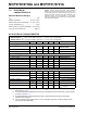
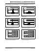
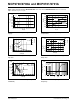
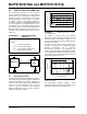
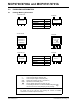
Table Of Contents
- 1.0 Electrical Characteristics
- 2.0 Typical Performance Curves
- FIGURE 2-1: Accuracy vs. Ambient Temperature (MCP9700A/9701A).
- FIGURE 2-2: Accuracy vs. Ambient Temperature, with VDD.
- FIGURE 2-3: Supply Current vs. Temperature.
- FIGURE 2-4: Accuracy vs. Ambient Temperature (MCP9700/9701).
- FIGURE 2-5: Changes in Accuracy vs. Ambient Temperature (Due to Load).
- FIGURE 2-6: Load Regulation vs. Ambient Temperature.
- FIGURE 2-7: Output Voltage at 0˚C (MCP9700/9700A).
- FIGURE 2-8: Occurrences vs. Temperature Coefficient (MCP9700/9700A).
- FIGURE 2-9: Power Supply Rejection (D˚C/DVDD) vs. Ambient Temperature.
- FIGURE 2-10: Output Voltage at 0˚C (MCP9701/9701A).
- FIGURE 2-11: Occurrences vs. Temperature Coefficient (MCP9701/9701A).
- FIGURE 2-12: Power Supply Rejection (D˚C/DVDD) vs. Temperature.
- FIGURE 2-13: Output Voltage vs. Power Supply.
- FIGURE 2-14: Output vs. Settling Time to step VDD.
- FIGURE 2-15: Thermal Response (Air to Fluid Bath).
- FIGURE 2-16: Output Voltage vs. Ambient Temperature.
- FIGURE 2-17: Output vs. Settling Time to Ramp VDD.
- FIGURE 2-18: Output Impedance vs. Frequency.
- 3.0 Pin Descriptions
- 4.0 Applications Information
- 5.0 Packaging Information

MCP9700/9700A and MCP9701/9701A
DS21942D-page 4 © 2007 Microchip Technology Inc.
2.0 TYPICAL PERFORMANCE CURVES
Note: Unless otherwise indicated, MCP9700/9700A: V
DD
= 2.3V to 5.5V; MCP9701/9701A: V
DD
= 3.1V to 5.5V;
GND = Ground, C
bypass
= 0.1 µF.
FIGURE 2-1: Accuracy vs. Ambient
Temperature (MCP9700A/9701A).
FIGURE 2-2: Accuracy vs. Ambient
Temperature, with V
DD
.
FIGURE 2-3: Supply Current vs.
Temperature.
FIGURE 2-4: Accuracy vs. Ambient
Temperature (MCP9700/9701).
FIGURE 2-5: Changes in Accuracy vs.
Ambient Temperature (Due to Load).
FIGURE 2-6: Load Regulation vs.
Ambient Temperature.
Note: The graphs and tables provided following this note are a statistical summary based on a limited number of
samples and are provided for informational purposes only. The performance characteristics listed herein
are not tested or guaranteed. In some graphs or tables, the data presented may be outside the specified
operating range (e.g., outside specified power supply range) and therefore outside the warranted range.
-2.0
-1.0
0.0
1.0
2.0
3.0
4.0
-50 -25 0 25 50 75 100 125
T
A
(°C)
Accuracy (°C)
MCP9700A
V
DD
= 3.3V
MCP9701A
V
DD
= 5.0V
Spec. Limits
-4.0
-2.0
0.0
2.0
4.0
6.0
-50 -25 0 25 50 75 100 125
T
A
(°C)
Accuracy (°C)
MCP9700/
MCP9700A
V
DD
= 5.5V
V
DD
= 2.3V
MCP9701/
MCP9701A
V
DD
= 5.5V
V
DD
= 3.1V
0.0
2.0
4.0
6.0
8.0
10.0
12.0
-50 -25 0 25 50 75 100 125
T
A
(°C)
I
DD
(µA)
MCP9700
MCP9700A
MCP9701
MCP9701A
-4.0
-2.0
0.0
2.0
4.0
6.0
-50 -25 0 25 50 75 100 125
T
A
(°C)
Accuracy (°C)
MCP9700
V
DD
= 3.3V
MCP9701
V
DD
= 5.0V
Spec. Limits
-0.2
-0.1
0
0.1
0.2
-50 -25 0 25 50 75 100 125
T
A
(°C)
Δ Accuracy Due to Load
(°C)
MCP9701/MCP9701A
V
DD
= 5.0V
MCP9700/MCP9700A
V
DD
= 3.3V
I
LOAD
= 100 µA
0.0
1.0
2.0
3.0
4.0
-50 -25 0 25 50 75 100 125
T
A
(°C)
Load Regulation ΔV/ΔI (Ω)
MCP9700/MCP9700A
MCP9701/MCP9701A
V
DD
= 3.3V
I
OUT
= 50 µA
I
OUT
= 100 µA
I
OUT
= 200 µA