
MCP9700 Specifications
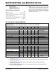
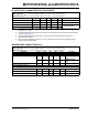
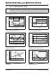
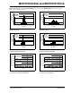
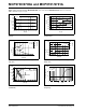
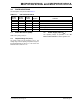
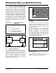
Table Of Contents
- 1.0 Electrical Characteristics
- 2.0 Typical Performance Curves
- FIGURE 2-1: Accuracy vs. Ambient Temperature (MCP9700A/9701A).
- FIGURE 2-2: Accuracy vs. Ambient Temperature, with VDD.
- FIGURE 2-3: Supply Current vs. Temperature.
- FIGURE 2-4: Accuracy vs. Ambient Temperature (MCP9700/9701).
- FIGURE 2-5: Changes in Accuracy vs. Ambient Temperature (Due to Load).
- FIGURE 2-6: Load Regulation vs. Ambient Temperature.
- FIGURE 2-7: Output Voltage at 0˚C (MCP9700/9700A).
- FIGURE 2-8: Occurrences vs. Temperature Coefficient (MCP9700/9700A).
- FIGURE 2-9: Power Supply Rejection (D˚C/DVDD) vs. Ambient Temperature.
- FIGURE 2-10: Output Voltage at 0˚C (MCP9701/9701A).
- FIGURE 2-11: Occurrences vs. Temperature Coefficient (MCP9701/9701A).
- FIGURE 2-12: Power Supply Rejection (D˚C/DVDD) vs. Temperature.
- FIGURE 2-13: Output Voltage vs. Power Supply.
- FIGURE 2-14: Output vs. Settling Time to step VDD.
- FIGURE 2-15: Thermal Response (Air to Fluid Bath).
- FIGURE 2-16: Output Voltage vs. Ambient Temperature.
- FIGURE 2-17: Output vs. Settling Time to Ramp VDD.
- FIGURE 2-18: Output Impedance vs. Frequency.
- 3.0 Pin Descriptions
- 4.0 Applications Information
- 5.0 Packaging Information

© 2007 Microchip Technology Inc. DS21942D-page 3
MCP9700/9700A and MCP9701/9701A
M
Turn-on Time t
ON
—800— µs
Typical Load Capacitance (Note 3)C
LOAD
— — 1000 pF
SC-70 Thermal Response to 63% t
RES
— 1.3 — s 30°C (Air) to +125°C
(Fluid Bath) (Note 4)
TO-92 Thermal Response to 63% t
RES
—1.65— s
DC ELECTRICAL CHARACTERISTICS (CONTINUED)
Electrical Specifications: Unless otherwise indicated:
MCP9700/9700A: V
DD
= 2.3V to 5.5V, GND = Ground, T
A
= -40°C to +125°C and No load.
MCP9701/9701A: V
DD
= 3.1V to 5.5V, GND = Ground, T
A
= -10°C to +125°C and No load.
Parameter Sym Min Typ Max Unit Conditions
Note 1: The MCP9700/9700A family accuracy is tested with V
DD
= 3.3V, while the MCP9701/9701A accuracy is
tested with V
DD
= 5.0V.
2: The MCP9700/9700A and MCP9701/9701A family is characterized using the first-order or linear equation,
as shown in Equation 4-2.
3: The MCP9700/9700A and MCP9701/9701A family is characterized and production tested with a
capacitive load of 1000 pF.
4: SC-70-5 package thermal response with 1x1 inch, dual-sided copper clad, TO-92-3 package thermal
response without PCB (leaded).
TEMPERATURE CHARACTERISTICS
Electrical Specifications: Unless otherwise indicated:
MCP9700/9700A: V
DD
= 2.3V to 5.5V, GND = Ground, T
A
= -40°C to +125°C and No load.
MCP9701/9701A: V
DD
= 3.1V to 5.5V, GND = Ground, T
A
= -10°C to +125°C and No load.
Parameters Sym Min Typ Max Units Conditions
Temperature Ranges
Specified Temperature Range T
A
-40 — +125 °C MCP9700/9700A
(Note)
T
A
-10 — +125 °C MCP9701/9701A
(Note)
Operating Temperature Range T
A
-40 — +125 °C
Storage Temperature Range T
A
-65 — +150 °C
Thermal Package Resistances
Thermal Resistance, 5LD SC-70 θ
JA
—331— °C/W
Thermal Resistance, 3LD SOT-23 θ
JA
—336— °C/W
Thermal Resistance, 3LD TO-92 θ
JA
— 131.9 — °C/W
Note: Operation in this range must not cause T
J
to exceed Maximum Junction Temperature (+150°C).