
MCP9700 Specifications
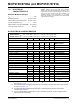
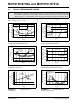
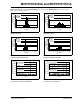
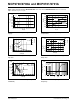
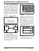
Table Of Contents
- 1.0 Electrical Characteristics
- 2.0 Typical Performance Curves
- FIGURE 2-1: Accuracy vs. Ambient Temperature (MCP9700A/9701A).
- FIGURE 2-2: Accuracy vs. Ambient Temperature, with VDD.
- FIGURE 2-3: Supply Current vs. Temperature.
- FIGURE 2-4: Accuracy vs. Ambient Temperature (MCP9700/9701).
- FIGURE 2-5: Changes in Accuracy vs. Ambient Temperature (Due to Load).
- FIGURE 2-6: Load Regulation vs. Ambient Temperature.
- FIGURE 2-7: Output Voltage at 0˚C (MCP9700/9700A).
- FIGURE 2-8: Occurrences vs. Temperature Coefficient (MCP9700/9700A).
- FIGURE 2-9: Power Supply Rejection (D˚C/DVDD) vs. Ambient Temperature.
- FIGURE 2-10: Output Voltage at 0˚C (MCP9701/9701A).
- FIGURE 2-11: Occurrences vs. Temperature Coefficient (MCP9701/9701A).
- FIGURE 2-12: Power Supply Rejection (D˚C/DVDD) vs. Temperature.
- FIGURE 2-13: Output Voltage vs. Power Supply.
- FIGURE 2-14: Output vs. Settling Time to step VDD.
- FIGURE 2-15: Thermal Response (Air to Fluid Bath).
- FIGURE 2-16: Output Voltage vs. Ambient Temperature.
- FIGURE 2-17: Output vs. Settling Time to Ramp VDD.
- FIGURE 2-18: Output Impedance vs. Frequency.
- 3.0 Pin Descriptions
- 4.0 Applications Information
- 5.0 Packaging Information

MCP9700/9700A and MCP9701/9701A
DS21942D-page 2 © 2007 Microchip Technology Inc.
1.0 ELECTRICAL
CHARACTERISTICS
Absolute Maximum Ratings †
V
DD
:...................................................................... 6.0V
Storage temperature: ........................ -65°C to +150°C
Ambient Temp. with Power Applied:.. -40°C to +125°C
Junction Temperature (T
J
):................................. 150°C
ESD Protection On All Pins (HBM:MM):.... (4 kV:200V)
Latch-Up Current at Each Pin: ...................... ±200 mA
†Notice: Stresses above those listed under “Maximum
Ratings” may cause permanent damage to the device. This is
a stress rating only and functional operation of the device at
those or any other conditions above those indicated in the
operational listings of this specification is not implied.
Exposure to maximum rating conditions for extended periods
may affect device reliability.
DC ELECTRICAL CHARACTERISTICS
Electrical Specifications: Unless otherwise indicated:
MCP9700/9700A: V
DD
= 2.3V to 5.5V, GND = Ground, T
A
= -40°C to +125°C and No load.
MCP9701/9701A: V
DD
= 3.1V to 5.5V, GND = Ground, T
A
= -10°C to +125°C and No load.
Parameter Sym Min Typ Max Unit Conditions
Power Supply
Operating Voltage Range V
DD
V
DD
2.3
3.1
—
—
5.5
5.5
V
V
MCP9700/9700A
MCP9701/9701A
Operating Current I
DD
—612µA
Power Supply Rejection Δ°C/ΔV
DD
—0.1—°C/V
Sensor Accuracy (Notes 1, 2)
T
A
= +25°C T
ACY
—±1—°C
T
A
= 0°C to +70°C T
ACY
-2.0 ±1 +2.0 °C MCP9700A/9701A
T
A
= -40°C to +125°C T
ACY
-2.0 ±1 +4.0 °C MCP9700A
T
A
= -10°C to +125°C T
ACY
-2.0 ±1 +4.0 °C MCP9701A
T
A
= 0°C to +70°C T
ACY
-4.0 ±2 +4.0 °C MCP9700/9701
T
A
= -40°C to +125°C T
ACY
-4.0 ±2 +6.0 °C MCP9700
T
A
= -10°C to +125°C T
ACY
-4.0 ±2 +6.0 °C MCP9701
Sensor Output
Output Voltage, T
A
= 0°C V
0°C
—500—mVMCP9700/9700A
Output Voltage, T
A
= 0°C V
0°C
—400—mVMCP9701/9701A
Temperature Coefficient T
C
—10.0—mV/°CMCP9700/9700A
T
C
—19.5—mV/°CMCP9701/9701A
Output Non-linearity V
ONL
—±0.5— °CT
A
= 0°C to +70°C (Note 2)
Output Current I
OUT
— — 100 µA
Output Impedance Z
OUT
—20—Ω I
OUT
= 100 µA, f = 500 Hz
Output Load Regulation ΔV
OUT
/
ΔI
OUT
—1—Ω T
A
= 0°C to +70°C,
I
OUT
= 100 µA
Note 1: The MCP9700/9700A family accuracy is tested with V
DD
= 3.3V, while the MCP9701/9701A accuracy is
tested with V
DD
= 5.0V.
2: The MCP9700/9700A and MCP9701/9701A family is characterized using the first-order or linear equation,
as shown in Equation 4-2.
3: The MCP9700/9700A and MCP9701/9701A family is characterized and production tested with a
capacitive load of 1000 pF.
4: SC-70-5 package thermal response with 1x1 inch, dual-sided copper clad, TO-92-3 package thermal
response without PCB (leaded).