
Datasheet

PCA9615 All information provided in this document is subject to legal disclaimers. © NXP Semiconductors N.V. 2016. All rights reserved.
Product data sheet Rev. 1.1 — 10 May 2016 8 of 29
NXP Semiconductors
PCA9615
2-channel multipoint Fm+ dI
2
C-bus buffer with hot-swap logic
7.4 Hot swap and power-on reset
During a power-on sequence, an initialization circuit holds the PCA9615 in a disconnected
state, meaning all outputs — SDA, SCL and the differential pins DSCLP/DSCLM and
DSDAP/DSDAM — are in a high-impedance state. As the power supply rises (either
power-up or live insertion), the initialization circuit enters a state where the internal
references are stabilized and an internal timer is triggered. After 1 ms, power is applied to
the rest of the circuitry and the PCA9615 detects the status on the differential
DSCLP/DSCLM and DSDAP/DSDAM lines. When the differential lines are detected as
connected to a bus with valid termination, that is, both DSCLM/DSDAM < 0.9 V
DD(B)
and
DSCLP/DSDAP > 0.1 V
DD(B)
, another timer is triggered. At the end of 10 ms, hot-swap
logic (Figure 2
) is enabled and the EN pin can detect a Stop Bit and Bus Idle condition.
However, there is still no connection between SDA and DSDAP/DSDAM or between SCL
and DSCLP/DSCLM. A successful EN pin sequence must occur for actual connection.
When the EN pin is set HIGH and the DSDAP and DSCLP pins have been HIGH for the
bus idle time or when both the SCL and SDA pins are HIGH and a STOP condition has
been seen on the differential bus (DSDAP/DSDAM and DSCLP/DSCLM pins), a
connection is established between the differential and the single-ended buses. Whenever
disconnected status is detected or the device is unpowered, the PCA9615 disconnects
the single-ended to differential buses, and the hot swap sequence repeats again before
the PCA9615 connects SDA to DSDAP/DSDAM and SCL to DSCLP/DSCLM.
Remark: Start-up process is the same for both PCA9616PW and PCA9615DP, except
that PIDET
and READY signals are only available in 16-pin package.
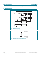
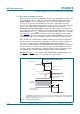
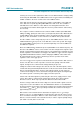
For PCA9615, the ready time is at least 11 ms (1 ms for power ready, 10 ms for plug-in debouncing
delay), which means the device can only be in operation after 11 ms with V
DD(A)
,V
DD(B)
ON and a
bus idle/stop detected; t
idle
= 100 s
Fig 6. Hot swap related timings
~11 ms
~1 ms
t
en
for power-on
and stabilization
V
DD(A)
, V
DD(B)
pwon
~10 ms
100 μs
EN
only when EN goes HIGH,
11 ms after plug-in,
will the bus idle/stop detector
start functioning
t
idle
SCL/SDA,
DSCL/DSDA
t
stop
connect differential
to single-ended bus
002aah774
plug-in debouncing time
not allowed