
Datasheet

PCA9615 All information provided in this document is subject to legal disclaimers. © NXP Semiconductors N.V. 2016. All rights reserved.
Product data sheet Rev. 1.1 — 10 May 2016 7 of 29
NXP Semiconductors
PCA9615
2-channel multipoint Fm+ dI
2
C-bus buffer with hot-swap logic
7.2.1 Noise rejection
Impulse noise coupled into the I
2
C-bus/SMBus signals can prevent the I
2
C-bus/SMBus
bus from operating reliably. The hostile signals may appear on the SCL line, SDA line, or
both. Impulse noise may also enter the common ground connection, or be caused by
current in the ground path caused by DC power supplies, or other signals sharing the
common ground return path. This problem is removed by using a differential transmission
line, in place of the I
2
C-bus/SMBus signal path. The dI
2
C-bus receiver (at each dI
2
C-bus
node) subtracts the signals on the two differential lines (D+ and D), and eliminates any
common-mode noise that is coupled into the dI
2
C-bus. The receiver amplifies the signals
which are also attenuated by the bulk resistance of the transmission line cable
connection, and does not rely on a common ground connection at each node.
7.2.2 Rejection of ground offset voltage
Hostile signals interfere with the I
2
C-bus/SMBus bus through the common ground
connection between each node. Current in this ground path causes an offset that may
cause false data or push the I
2
C-bus/SMBus signals outside of an acceptable range.
Unwanted ground offset can be caused by heavy DC current in the ground path, or
injection of ground current from AC signals, either of which may show up as false signals.
Because the dI
2
C-bus node receiver responds only to the difference between the two
dI
2
C-bus transmission lines, common-mode signals are ignored. There is no need to have
a ground connection between each of the nodes, which may be powered locally. Nodes
may also be powered by extra conductors (for V
DD
and ground) run with the dI
2
C-bus
signals. Voltage offsets caused by DC current in these additional wires are ignored by the
dI
2
C-bus receiver, which subtracts the two differential signals (D+ and D).
7.3 EN pin
Enable input to connect the device into the bus. When this pin is LOW, the device never
connects to the bus, and disconnect the SCL/SDA from differential SCL/SDA. When EN is
driven HIGH, and V
DD(A)
and V
DD(B)
are stable, the EN pin connects SDA/SCL to
differential SDA/SCL after a stop bit or bus idle has been detected on differential line bus.
It should never change state during an I
2
C-bus/SMBus operation because disabling
during a bus operation hangs the bus and enabling part way through a bus cycle could
confuse the I
2
C-bus/SMBus parts being enabled. The EN pin should only change state
when the global bus and the buffer port are in an idle state to prevent system failures.
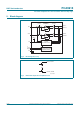
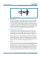
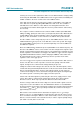
Fig 5. dI
2
C-bus terminations
DxxxP
DxxxM
aaa-011061
twisted-pair cable
DxxxP
DxxxM