
Datasheet

PCA9615 All information provided in this document is subject to legal disclaimers. © NXP Semiconductors N.V. 2016. All rights reserved.
Product data sheet Rev. 1.1 — 10 May 2016 6 of 29
NXP Semiconductors
PCA9615
2-channel multipoint Fm+ dI
2
C-bus buffer with hot-swap logic
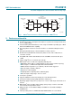
7. Functional description
Refer to Figure 2.
The PCA9615 is used at each node of the dI
2
C-bus signal path, to provide conversion
from the dI
2
C-bus signal format to conventional I
2
C-bus/SMBus, allowing the connection
of existing I
2
C-bus/SMBus devices as slaves or the bus master. Because the signal
voltages on the I
2
C-bus/SMBus bus side may be different from the dI
2
C-bus side, there
are two power supply pins and a common ground. To prevent bus latch-up, the
I
2
C-bus/SMBus side employs static offset. Signal direction is determined by the
I
2
C-bus/SMBus bus protocol, and does not require a direction signal, as these bus buffers
automatically set signal flow direction. An enable pin (EN) is provided to disable the bus
buffer, and is useful for fault finding, power-up sequencing, or reconfiguration of a large
bus system by isolating sections not needed at all times.
Construction of the differential transmission line is not device-dependent. PCB traces,
open wiring, twisted-pair cables or a combination of these may be used. Twisted-pair
cables offer the best performance. A typical twisted-pair transmission line cable has a
characteristic impedance of ‘about 100 ’ and must be terminated at both ends in 100
to prevent unwanted signal reflections. Multiple nodes (each using a dI
2
C-bus buffer) may
be connected at any point along this transmission line, however, the stub length degrades
the bus performance, and should therefore be minimized.
7.1 I
2
C-bus/SMBus side
The I
2
C-bus/SMBus side of the PCA9615 differential bus buffer is connected to other
I
2
C-bus/SMBus devices and requires pull-up resistors on each of the SCL and SDA
signals. The value of the resistor should be chosen based on the bus capacitance and
desired data speed, being careful not to overload the driver current rating of 3 mA for
Standard and Fast modes, 30 mA for Fast-mode Plus (Fm+). The I
2
C-bus/SMBus side of
the PCA9615 is powered from the V
DD(A)
supply pin.
7.2 dI
2
C-bus side differential pair
In previous I
2
C-bus/SMBus designs, the nodes (Master and one or more Slaves) are
connected by wired-OR in combination with a single pull-up resistor. This simple
arrangement is not suited for long distances more than 1 meter (1 m) or about 3 feet (3 ft),
due to ringing and reflections on the un-terminated bus. The use of a transmission line
with correct termination eliminates this problem, and is further improved by differential
signaling used in the dI
2
C-bus scheme. Each node acts as both a driver and a receiver to
allow bidirectional signal flow, but not at the same time. Switching from transmit to receive
is done automatically. The dI
2
C-bus side of the PCA9615 is powered from the V
DD(B)
supply pin.
The dI
2
C-bus is also biased to an idle state (D+ more positive than D) to be compatible
with the I
2
C-bus/SMBus wired-OR scheme, when not transmitting traffic (data). This
allows every node to receive broadcast messages from the Master, and return ACK/NACK
and data in response. Biasing is done with additional resistors, connected to V
DD(B)
and
V
SS
(the local ground), as shown in Figure 5. The transmission line is terminated in the
characteristic impedance of the cable, typically 100 . This is the value defined by three
resistors, the other two resistors providing the idle condition bias to the twisted pair.