
Datasheet

NXP Semiconductors
PCA9615
2-channel multipoint Fm+ dI
2
C-bus buffer with hot-swap logic
© NXP Semiconductors N.V. 2016. All rights reserved.
For more information, please visit: http://www.nxp.com
For sales office addresses, please send an email to: salesaddresses@nxp.com
Date of release: 10 May 2016
Document identifier: PCA9615
Please be aware that important notices concerning this document and the product(s)
described herein, have been included in section ‘Legal information’.
20. Contents
1 General description. . . . . . . . . . . . . . . . . . . . . . 1
2 Features and benefits . . . . . . . . . . . . . . . . . . . . 2
3 Applications . . . . . . . . . . . . . . . . . . . . . . . . . . . . 3
4 Ordering information. . . . . . . . . . . . . . . . . . . . . 3
4.1 Ordering options. . . . . . . . . . . . . . . . . . . . . . . . 3
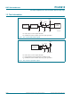
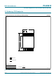
5 Block diagram . . . . . . . . . . . . . . . . . . . . . . . . . . 4
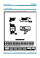
6 Pinning information. . . . . . . . . . . . . . . . . . . . . . 5
6.1 Pinning . . . . . . . . . . . . . . . . . . . . . . . . . . . . . . . 5
6.2 Pin description . . . . . . . . . . . . . . . . . . . . . . . . . 5
7 Functional description . . . . . . . . . . . . . . . . . . . 6
7.1 I
2
C-bus/SMBus side . . . . . . . . . . . . . . . . . . . . . 6
7.2 dI
2
C-bus side differential pair . . . . . . . . . . . . . . 6
7.2.1 Noise rejection . . . . . . . . . . . . . . . . . . . . . . . . . 7
7.2.2 Rejection of ground offset voltage . . . . . . . . . . 7
7.3 EN pin. . . . . . . . . . . . . . . . . . . . . . . . . . . . . . . . 7
7.4 Hot swap and power-on reset. . . . . . . . . . . . . . 8
8 Application design-in information . . . . . . . . . . 9
8.1 I
2
C-bus . . . . . . . . . . . . . . . . . . . . . . . . . . . . . . . 9
8.2 Differential I
2
C-bus application . . . . . . . . . . . . . 9
9 Limiting values. . . . . . . . . . . . . . . . . . . . . . . . . 16
10 Static characteristics. . . . . . . . . . . . . . . . . . . . 17
11 Dynamic characteristics . . . . . . . . . . . . . . . . . 18
11.1 AC waveforms . . . . . . . . . . . . . . . . . . . . . . . . 19
12 Test information. . . . . . . . . . . . . . . . . . . . . . . . 20
13 Package outline . . . . . . . . . . . . . . . . . . . . . . . . 21
14 Soldering of SMD packages . . . . . . . . . . . . . . 22
14.1 Introduction to soldering . . . . . . . . . . . . . . . . . 22
14.2 Wave and reflow soldering . . . . . . . . . . . . . . . 22
14.3 Wave soldering. . . . . . . . . . . . . . . . . . . . . . . . 22
14.4 Reflow soldering. . . . . . . . . . . . . . . . . . . . . . . 23
15 Soldering: PCB footprints. . . . . . . . . . . . . . . . 25
16 Abbreviations. . . . . . . . . . . . . . . . . . . . . . . . . . 26
17 Revision history. . . . . . . . . . . . . . . . . . . . . . . . 26
18 Legal information. . . . . . . . . . . . . . . . . . . . . . . 27
18.1 Data sheet status . . . . . . . . . . . . . . . . . . . . . . 27
18.2 Definitions. . . . . . . . . . . . . . . . . . . . . . . . . . . . 27
18.3 Disclaimers . . . . . . . . . . . . . . . . . . . . . . . . . . . 27
18.4 Trademarks. . . . . . . . . . . . . . . . . . . . . . . . . . . 28
19 Contact information. . . . . . . . . . . . . . . . . . . . . 28
20 Contents . . . . . . . . . . . . . . . . . . . . . . . . . . . . . . 29