
Datasheet


PCA9615 All information provided in this document is subject to legal disclaimers. © NXP Semiconductors N.V. 2016. All rights reserved.
Product data sheet Rev. 1.1 — 10 May 2016 20 of 29
NXP Semiconductors
PCA9615
2-channel multipoint Fm+ dI
2
C-bus buffer with hot-swap logic
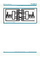
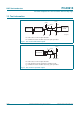
12. Test information
R
L
= load resistor; 1.35 k on single-ended side.
R
T
= termination resistance should be equal to Z
o
of pulse generators.
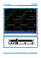
Fig 16. Test circuit for differential outputs
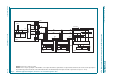
R
L
= load resistor; 1.35 k on single-ended side.
C
L
= load capacitance includes jig and probe capacitance; 50 pF.
R
T
= termination resistance should be equal to Z
o
of pulse generators.
Fig 17. Test circuit for open-drain output
I
2
C-BUS
LEVEL SHIFTER
V
O
60 Ω
002aag419
R
T
V
I
V
DD(B)
DUT
V
DD(A)
PULSE
GENERATOR
300 Ω
V
DD(A)
P
M
300 Ω
V
DD(B)
DIFFERENTIAL
PROBE
DIFFERENTIAL
V
O
C
L
R
L
002aag420
R
T
V
DD(A)
V
DD(A)
DUT
V
DD(B)
P
M