
Datasheet


PCA9615 All information provided in this document is subject to legal disclaimers. © NXP Semiconductors N.V. 2016. All rights reserved.
Product data sheet Rev. 1.1 — 10 May 2016 19 of 29
NXP Semiconductors
PCA9615
2-channel multipoint Fm+ dI
2
C-bus buffer with hot-swap logic
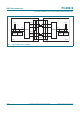
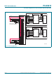
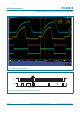
11.1 AC waveforms
V
DD(A)
=3.0V.
SR
f
=0.6 (V
high
V
low
) / t
THL
SR
r
=0.6 (V
high
V
low
) / t
TLH
V
DD(A)
=3.0V.
SR
f
=0.6´V
DD(A)
/ t
THL
Fig 13. Propagation delay and transition times;
single-ended side to differential side
Fig 14. Propagation delay and transition times;
differential side to single-ended side
Fig 15. Propagation delay
002aag416
V
DD(A)
0.3 V
t
PLH
t
THL
0.5V
DD(A)
0.5V
DD(A)
input
output
20 %
0 V
0 V
80 %
20 %
80 %
t
PHL
t
TLH
−2.5 V
0.1 V
differential
voltage
input
output
80 %
80 %
0.5V
DD(A)
0.5V
DD(A)
20 %20 %
0 V 0 V
t
PHL
t
PLH
0.3 V
−0.3 V
V
DD(A)
t
THL
t
TLH
002aag417
differential
voltage
0.5 V
input
SDA, SCL
output
DSCLP/DSCLM,
DSDAP/DSDAM
t
PLH2
0 V
002aag418
0.3 V
−2.5 V
0.5V
DD(A)
t
PLH