
Datasheet


PCA9615 All information provided in this document is subject to legal disclaimers. © NXP Semiconductors N.V. 2016. All rights reserved.
Product data sheet Rev. 1.1 — 10 May 2016 18 of 29
NXP Semiconductors
PCA9615
2-channel multipoint Fm+ dI
2
C-bus buffer with hot-swap logic
[1] LOW-level supply voltage.
11. Dynamic characteristics
[1] Times are specified with loads of 1.35 k pull-up resistance and 50 pF load capacitance on the A side, and 50 termination network
resistance and 50 pF load capacitance on the B side. Different load resistance and capacitance alters the RC time constant, thereby
changing the propagation delay and transition times.
[2] Pull-up voltages are V
DD(A)
on the A side and termination network on the B side.
[3] Typical values were measured with V
DD(A)
= 3.3 V at T
amb
=25C, unless otherwise noted.
[4] The t
PLH
delay data from B side to A side is measured at 0 V differential on the B side to 0.5V
DD(A)
on the A side.
[5] Typical value measured with V
DD(A)
=3.3V at T
amb
=25C.
[6] The proportional delay data from A side to B side is measured at 0.5V
DD(A)
on the A side to 0 V on the B side.
[7] The enable pin (EN) should only change state when the global bus and the repeater port are in an idle state.
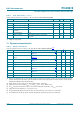
Input EN
V
IH
HIGH-level input voltage 0.7V
DD(A)
-5.5 V
V
IL
LOW-level input voltage 0.5 - +0.3V
DD(A)
V
I
LI
input leakage current V
I
=V
DD(B)
1-+1 A
I
IL(EN)
LOW-level input current
on pin EN
V
I
= 0.2 V, EN; V
DD(A)
=5.5V - 20 54 A
C
i
input capacitance V
I
=V
DD(A)
-610pF
R
PU
pull-up resistance internal pull-up resistor connected to
V
DD(A)
rail
- 300 - k
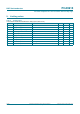
Table 5. Static characteristics …continued
V
DD(B)
= 3.0 V to 5.5 V; V
SS
=0V; T
amb
=
40
C to +85
C; unless otherwise specified.
Symbol Parameter Conditions Min Typ Max Unit
Table 6. Dynamic characteristics
V
DD
= 2.7 V to 5.5 V; V
SS
=0V; T
amb
=
40
C to +85
C; unless otherwise specified.
[1][2]
Symbol Parameter Conditions Min Typ
[3]
Max Unit
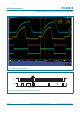
t
PLH
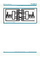
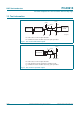
LOW to HIGH propagation delay single-ended side to differential side;
Figure 15
[4]
140 120 - ns
t
PLH2
LOW to HIGH propagation
delay 2
single-ended side to differential side;
Figure 15
--100ns
t
PHL
HIGH to LOW propagation delay single-ended side to differential side;
Figure 13
[5]
--120ns
SR
r
rising slew rate differential side; Figure 13 --1V/ns
SR
f
falling slew rate differential side; Figure 13
[5]
--1V/ns
t
PLH
LOW to HIGH propagation delay differential side to single-ended side;
Figure 14
[6]
--150ns
t
PHL
HIGH to LOW propagation delay differential side to single-ended side;
Figure 14
[6]
--150ns
SR
f
falling slew rate single-ended side; Figure 14 --0.1V/ns
t
dis
disable time EN LOW to disable
[7]
--200ns