
Datasheet


PCA9615 All information provided in this document is subject to legal disclaimers. © NXP Semiconductors N.V. 2016. All rights reserved.
Product data sheet Rev. 1.1 — 10 May 2016 17 of 29
NXP Semiconductors
PCA9615
2-channel multipoint Fm+ dI
2
C-bus buffer with hot-swap logic
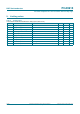
10. Static characteristics
Table 5. Static characteristics
V
DD(B)
= 3.0 V to 5.5 V; V
SS
=0V; T
amb
=
40
C to +85
C; unless otherwise specified.
Symbol Parameter Conditions Min Typ Max Unit
Supplies
V
DD(B)
supply voltage port B differential bus 3.0 - 5.5 V
V
DD(A)
supply voltage port A single-ended bus
[1]
2.3 - 5.5 V
I
DD(VDDA)
supply current on
pin V
DD(A)
--16A
I
DDH(B)
port B HIGH-level supply
current
both channels HIGH; V
DD(B)
=5.5V;
SDAn = SCLn = V
DD(A)
=5.5V
-0.81.6mA
I
DDL(B)
port B LOW-level supply
current
both channels LOW; V
DD(B)
=5.5V;
SDA and SCL = V
SS
; differential I/Os open
-1.11.8mA
driving termination; 2 channel - 70 91 mA
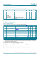
Input and output SDA and SCL
V
IH
HIGH-level input voltage 0.7V
DD(A)
-5.5 V
V
IL
LOW-level input voltage 0.5 - +0.4 V
V
IK
input clamping voltage I
I
= 18 mA 1.5 - 0 V
I
LI
input leakage current V
I
=V
DD(A)
--2 A
I
IL
LOW-level input current SDA, SCL; V
I
=0.2V - - 12 A
V
OL
LOW-level output voltage I
OL
=200A or 30 mA 0.47 0.52 0.6 V
V
OL
V
IL
difference between
LOW-level output and
LOW-level input voltage
guaranteed by design - - 90 mV
I
LOH
HIGH-level output leakage
current
V
O
=V
DD(A)
--2 A
C
io
input/output capacitance V
I
=V
DD(A)
or 0 V; disabled or V
DD(A)
=0V - 7 10 pF
Input and output DSDAP/DSDAM and DSCLP/DSCLM
V
cm
common-mode voltage 0 - V
DD(B)
V
I
LI
input leakage current V
I
=V
DD(B)
--40 A
I
IL
LOW-level input current V
I
=0.2V - - 40 A
R
PU
pull-up resistance internal pull-up resistor on DSCLM and
DSDAM connected to V
DD(B)
rail
- 200 - k
R
pd
pull-down resistance internal pull-down resistor on DSCLP and
DSDAP connected to V
SS
rail
- 200 - k
V
th(dif)
differential receiver
threshold voltage
0V V
cm
V
DD(B)
200 - +200 mV
V
I(hys)
hysteresis of input voltage receiver; 0 V V
cm
V
DD(B)
-30- mV
V
o(dif)(p-p)
peak-to-peak differential
output voltage
single-ended input LOW
no load V
DD(B)
-- V
R
L
= 54 at V
DD(B)
=5V 5.0 1.5 1.0 V
C
io
input/output capacitance V
I
=V
DD(B)
or 0 V; disabled or V
DD(B)
=0V - 7 10 pF