
Datasheet
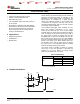
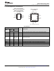
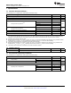
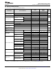
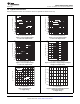

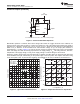
Table Of Contents
- 1 Features
- 2 Applications
- 3 Description
- 4 Simplified Schematic
- Table of Contents
- 5 Revision History
- 6 Pin Configuration and Functions
- 7 Specifications
- 8 Detailed Description
- 9 Applications and Implementation
- 10 Power Supply Recommendations
- 11 Device and Documentation Support
- 12 Mechanical, Packaging, and Orderable Information

1
2
3
4
8
7
6
5
GND
TRIG
OUT
RESET
V
CC
DISCH
THRES
CONT
3 2 1 20 19
9 10 11 12 13
4
5
6
7
8
18
17
16
15
14
NC
DISCH
NC
THRES
NC
NC
TRIG
NC
OUT
NC
NC
GND
NC
CONT
NC
V
CC
NC
NC
RESET
NC
NC – No internal connection
NA555...D OR P PACKAGE
NE555...D, P, PS, OR PW PACKAGE
SA555...D OR P PACKAGE
SE555...D, JG, OR P PACKAGE
(TOP VIEW)
SE555...FK PACKAGE
(TOP VIEW)
NA555
,
NE555
,
SA555
,
SE555
www.ti.com
SLFS022I –SEPTEMBER 1973–REVISED SEPTEMBER 2014
6 Pin Configuration and Functions
Pin Functions
PIN
D, P, PS,
FK I/O DESCRIPTION
PW, JG
NAME
NO.
Controls comparator thresholds, Outputs 2/3 VCC, allows bypass capacitor
CONT 5 12 I/O
connection
DISCH 7 17 O Open collector output to discharge timing capacitor
GND 1 2 – Ground
1, 3, 4, 6, 8,
9, 11, 13,
NC – No internal connection
14, 16, 18,
19
OUT 3 7 O High current timer output signal
RESET 4 10 I Active low reset input forces output and discharge low.
THRES 6 15 I End of timing input. THRES > CONT sets output low and discharge low
TRIG 2 5 I Start of timing input. TRIG < ½ CONT sets output high and discharge open
V
CC
8 20 – Input supply voltage, 4.5 V to 16 V. (SE555 maximum is 18 V)
Copyright © 1973–2014, Texas Instruments Incorporated Submit Documentation Feedback 3
Product Folder Links: NA555 NE555 SA555 SE555