
Datasheet
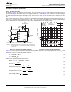
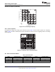

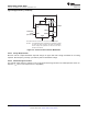

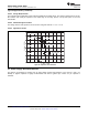


Table Of Contents
- 1 Features
- 2 Applications
- 3 Description
- 4 Simplified Schematic
- Table of Contents
- 5 Revision History
- 6 Pin Configuration and Functions
- 7 Specifications
- 8 Detailed Description
- 9 Applications and Implementation
- 10 Power Supply Recommendations
- 11 Device and Documentation Support
- 12 Mechanical, Packaging, and Orderable Information

Voltage − 5 V/div
t − Time − 1 s/div
ÏÏÏÏÏ
ÏÏÏÏÏ
ÏÏÏÏÏ
See Figure 22
ÏÏÏÏ
ÏÏÏÏ
ÏÏÏÏ
Output A
ÏÏÏÏ
ÏÏÏÏ
ÏÏÏÏ
ÏÏÏÏ
Output B
ÏÏÏÏ
ÏÏÏÏ
ÏÏÏÏ
Output C
ÏÏÏ
ÏÏÏ
ÏÏÏ
ÏÏÏ
t = 0
ÏÏÏÏÏ
ÏÏÏÏÏ
ÏÏÏÏÏ
t
w
C = 1.1 R
C
C
C
ÏÏ
ÏÏ
ÏÏ
t
w
C
ÏÏÏÏÏ
ÏÏÏÏÏ
ÏÏÏÏÏ
t
w
B = 1.1 R
B
C
B
ÏÏÏÏÏ
ÏÏÏÏÏ
ÏÏÏÏÏ
t
w
A = 1.1 R
A
C
A
ÏÏÏ
ÏÏÏ
ÏÏÏ
ÏÏÏ
t
w
A
ÏÏÏ
ÏÏÏ
ÏÏÏ
ÏÏÏ
t
w
B
NA555
,
NE555
,
SA555
,
SE555
SLFS022I –SEPTEMBER 1973–REVISED SEPTEMBER 2014
www.ti.com
Typical Applications (continued)
9.2.4.1 Design Requirements
The sequential timer application chains together multiple mono-stable timers. The joining components are the 33-
kΩ resistors and 0.001- µF capacitors. The output high to low edge passes a 10-µs start pulse to the next
monostable.
9.2.4.2 Detailed Design Procedure
The timing resistors and capacitors can be chosen using this formula. t
w
= 1.1 × R × C.
9.2.4.3 Application Curves
Figure 23. Sequential Timer Waveforms
10 Power Supply Recommendations
The devices are designed to operate from an input voltage supply range between 4.5 V and 16 V. (18 V for
SE555). A bypass capacitor is highly recommended from VCC to ground pin; ceramic 0.1 µF capacitor is
sufficient.
18 Submit Documentation Feedback Copyright © 1973–2014, Texas Instruments Incorporated
Product Folder Links: NA555 NE555 SA555 SE555