
Datasheet
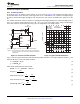
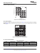

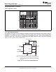
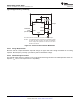

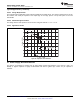


Table Of Contents
- 1 Features
- 2 Applications
- 3 Description
- 4 Simplified Schematic
- Table of Contents
- 5 Revision History
- 6 Pin Configuration and Functions
- 7 Specifications
- 8 Detailed Description
- 9 Applications and Implementation
- 10 Power Supply Recommendations
- 11 Device and Documentation Support
- 12 Mechanical, Packaging, and Orderable Information

Voltage − 2 V/div
Time − 0.5 ms/div
ÏÏÏÏÏÏ
ÏÏÏÏÏÏ
ÏÏÏÏÏÏ
Capacitor Voltage
ÏÏÏÏÏ
ÏÏÏÏÏ
ÏÏÏÏÏ
ÏÏÏÏÏ
Output Voltage
ÏÏÏÏÏÏ
ÏÏÏÏÏÏ
ÏÏÏÏÏÏ
ÏÏÏÏÏÏ
Clock Input Voltage
ÏÏÏÏÏ
ÏÏÏÏÏ
ÏÏÏÏÏ
ÏÏÏÏÏ
ÏÏÏÏÏ
ÏÏÏÏÏ
R
A
= 3 kΩ
C = 0.02 µF
R
L
= 1 kΩ
See Figure 18
ÏÏÏÏÏÏÏ
ÏÏÏÏÏÏÏ
ÏÏÏÏÏÏÏ
Modulation Input Voltage
NA555
,
NE555
,
SA555
,
SE555
www.ti.com
SLFS022I –SEPTEMBER 1973–REVISED SEPTEMBER 2014
Typical Applications (continued)
9.2.2.1 Design Requirements
Clock input must have V
OL
and V
OH
levels that are less than and greater than 1/3 VCC. Modulation input can
vary from ground to VCC. The application must be tolerant of a nonlinear transfer function; the relationship
between modulation input and pulse width is not linear because the capacitor charge is based RC on an negative
exponential curve.
9.2.2.2 Detailed Design Procedure
Choose R
A
and C so that R
A
× C = 1/4 [clock input period]. R
L
improves V
OH
, but it is not required for TTL
compatibility.
9.2.2.3 Application Curves
Figure 19. Pulse-Width-Modulation Waveforms
9.2.3 Pulse-Position Modulation
As shown in Figure 20, any of these timers can be used as a pulse-position modulator. This application
modulates the threshold voltage and, thereby, the time delay, of a free-running oscillator. Figure 21 shows a
triangular-wave modulation signal for such a circuit; however, any wave shape could be used.
Copyright © 1973–2014, Texas Instruments Incorporated Submit Documentation Feedback 15
Product Folder Links: NA555 NE555 SA555 SE555