
Datasheet

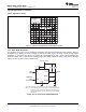
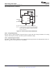


Table Of Contents
- 1 Features
- 2 Applications
- 3 Description
- 4 Simplified Schematic
- Table of Contents
- 5 Revision History
- 6 Pin Configuration and Functions
- 7 Specifications
- 8 Detailed Description
- 9 Applications and Implementation
- 10 Power Supply Recommendations
- 11 Device and Documentation Support
- 12 Mechanical, Packaging, and Orderable Information

V
CC
(5 V to 15 V)
DISCH
OUT
V
CC
RESET
R
L
R
A
A5T3644
C
THRES
GND
CONT
TRIG
Input
0.01 µF
ÎÎÎ
ÎÎÎ
ÎÎÎ
ÎÎÎ
Output
4 8
3
7
6
2
5
1
Pin numbers shown are shown for the D, JG, P, PS, and PW packages.
NA555
,
NE555
,
SA555
,
SE555
www.ti.com
SLFS022I –SEPTEMBER 1973–REVISED SEPTEMBER 2014
9 Applications and Implementation
NOTE
Information in the following applications sections is not part of the TI component
specification, and TI does not warrant its accuracy or completeness. TI’s customers are
responsible for determining suitability of components for their purposes. Customers should
validate and test their design implementation to confirm system functionality.
9.1 Application Information
The xx555 timer devices use resistor and capacitor charging delay to provide a programmable time delay or
operating frequency. This section presents a simplified discussion of the design process.
9.2 Typical Applications
9.2.1 Missing-Pulse Detector
The circuit shown in Figure 16 can be used to detect a missing pulse or abnormally long spacing between
consecutive pulses in a train of pulses. The timing interval of the monostable circuit is re-triggered continuously
by the input pulse train as long as the pulse spacing is less than the timing interval. A longer pulse spacing,
missing pulse, or terminated pulse train permits the timing interval to be completed, thereby generating an output
pulse as shown in Figure 17.
Figure 16. Circuit for Missing-Pulse Detector
9.2.1.1 Design Requirements
Input fault (missing pulses) must be input high. Input stuck low will not be detected because timing capacitor "C"
will remain discharged.
9.2.1.2 Detailed Design Procedure
Choose R
A
and C so that R
A
× C > [maximum normal input high time]. R
L
improves V
OH
, but it is not required for
TTL compatibility.
Copyright © 1973–2014, Texas Instruments Incorporated Submit Documentation Feedback 13
Product Folder Links: NA555 NE555 SA555 SE555