
Datasheet

1N4001, 1N4002, 1N4003, 1N4004, 1N4005, 1N4006, 1N4007
www.onsemi.com
2
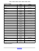
MAXIMUM RATINGS
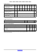
Rating Symbol 1N4001 1N4002 1N4003 1N4004 1N4005 1N4006 1N4007 Unit
†Peak Repetitive Reverse Voltage
Working Peak Reverse Voltage
DC Blocking Voltage
V
RRM
V
RWM
V
R
50 100 200 400 600 800 1000 V
†Non−Repetitive Peak Reverse Voltage
(halfwave, single phase, 60 Hz)
V
RSM
60 120 240 480 720 1000 1200 V
†RMS Reverse Voltage V
R(RMS)
35 70 140 280 420 560 700 V
†Average Rectified Forward Current
(single phase, resistive load,
60 Hz, T
A
= 75°C)
I
O
1.0 A
†Non−Repetitive Peak Surge Current
(surge applied at rated load conditions)
I
FSM
30 (for 1 cycle) A
Operating and Storage Junction
Temperature Range
T
J
T
stg
−65 to +175 °C
Stresses exceeding those listed in the Maximum Ratings table may damage the device. If any of these limits are exceeded, device functionality
should not be assumed, damage may occur and reliability may be affected.
†Indicates JEDEC Registered Data
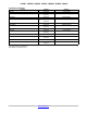
THERMAL CHARACTERISTICS
Rating Symbol Max Unit
Maximum Thermal Resistance, Junction−to−Ambient
R
q
JA
Note 1 °C/W
ELECTRICAL CHARACTERISTICS†
Rating Symbol Typ Max Unit
Maximum Instantaneous Forward Voltage Drop, (i
F
= 1.0 Amp, T
J
= 25°C) v
F
0.93 1.1 V
Maximum Full−Cycle Average Forward Voltage Drop, (I
O
= 1.0 Amp, T
L
= 75°C, 1 inch leads) V
F(AV)
− 0.8 V
Maximum Reverse Current (rated DC voltage)
(T
J
= 25°C)
(T
J
= 100°C)
I
R
0.05
1.0
10
50
mA
Maximum Full−Cycle Average Reverse Current, (I
O
= 1.0 Amp, T
L
= 75°C, 1 inch leads) I
R(AV)
− 30
mA
Product parametric performance is indicated in the Electrical Characteristics for the listed test conditions, unless otherwise noted. Product
performance may not be indicated by the Electrical Characteristics if operated under different conditions.
†Indicates JEDEC Registered Data