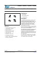
TSH80, TSH81, TSH82, TSH84 Wide-band rail-to-rail operational amplifiers with standby function Datasheet - production data Applications • Video buffers • A/D converter drivers SO8 SOT23-5 • Hi-fi applications Description TSSOP8 TSSOP14 Features • Operating range from 4.5 to 12 V • 3 dB-bandwidth: 100 MHz • Slew rate 100 V/µs • Output current up to 55 mA • Input single supply voltage • Output rail-to-rail • Specified for 150 Ω loads • Low distortion, THD 0.
Contents TSH80, TSH81, TSH82, TSH84 Contents 1 Package pin connections . . . . . . . . . . . . . . . . . . . . . . . . . . . . . . . . . . . . . 5 2 Absolute maximum ratings and operating conditions . . . . . . . . . . . . . 6 3 Electrical characteristics . . . . . . . . . . . . . . . . . . . . . . . . . . . . . . . . . . . . . 7 4 Test conditions . . . . . . . . . . . . . . . . . . . . . . . . . . . . . . . . . . . . . . . . . . . . 19 4.1 Layout precautions . . . . . . . . . . . . . . . . . . .
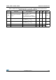
TSH80, TSH81, TSH82, TSH84 List of tables List of tables Table 1. Table 2. Table 3. Table 4. Table 5. Table 6. Table 7. Table 8. Table 9. Table 10. Table 11. Table 12. Table 13. Absolute maximum ratings . . . . . . . . . . . . . . . . . . . . . . . . . . . . . . . . . . . . . . . . . . . . . . . . . . 6 Operating conditions . . . . . . . . . . . . . . . . . . . . . . . . . . . . . . . . . . . . . . . . . . . . . . . . . . . . . . . 6 Electrical characteristics at VCC+ = +5 V, VCC- = GND, Vic = 2.
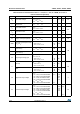
List of figures TSH80, TSH81, TSH82, TSH84 List of figures Figure 1. Figure 2. Figure 3. Figure 4. Figure 5. Figure 6. Figure 7. Figure 8. Figure 9. Figure 10. Figure 11. Figure 12. Figure 13. Figure 16. Figure 14. Figure 15. Figure 17. Figure 18. Figure 19. Figure 20. Figure 21. Figure 22. Figure 23. Figure 24. Figure 25. Figure 26. Figure 27. Figure 28. Figure 31. Figure 29. Figure 30. Figure 32. Figure 33. Figure 34. Figure 35. Figure 36. Figure 37. Figure 38. Figure 39.
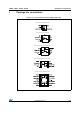
TSH80, TSH81, TSH82, TSH84 1 Package pin connections Package pin connections Figure 1.
Absolute maximum ratings and operating conditions 2 TSH80, TSH81, TSH82, TSH84 Absolute maximum ratings and operating conditions Table 1.
TSH80, TSH81, TSH82, TSH84 3 Electrical characteristics Electrical characteristics Table 3. Electrical characteristics at VCC+ = +5 V, VCC- = GND, Vic = 2.5 V, Tamb = 25 °C (unless otherwise specified) Symbol Parameter Test conditions Min. Typ. Max. Unit 10 12 mV Input offset voltage Tamb = 25 °C Tmin < Tamb < Tmax 1.1 Input offset voltage drift vs. temperature Tmin < Tamb < Tmax 3 Iio Input offset current Tamb = 25 °C Tmin < Tamb < Tmax 0.1 3.
Electrical characteristics TSH80, TSH81, TSH82, TSH84 Table 3. Electrical characteristics at VCC+ = +5 V, VCC- = GND, Vic = 2.5 V, Tamb = 25 °C (unless otherwise specified) (continued) Symbol Voh Vol GBP Bw SR Parameter High-level output voltage Low-level output voltage Gain bandwidth product Test conditions Tamb = 25 °C RL = 150 Ω connected to GND RL = 600 Ω connected to GND RL = 2 kΩ connected to GND RL = 10 kΩ connected to GND RL = 150 Ω connected to 2.5 V RL = 600 Ω connected to 2.
TSH80, TSH81, TSH82, TSH84 Electrical characteristics Table 3. Electrical characteristics at VCC+ = +5 V, VCC- = GND, Vic = 2.5 V, Tamb = 25 °C (unless otherwise specified) (continued) Symbol Parameter Test conditions Min. Typ. Max. Unit IM3 Third order intermodulation product AVCL = +2, Vout = 2 Vpp RL = 150 Ω to 2.5 V Fin1 = 180 kHz, Fin2 = 280 kHz spurious measurement at 400 kHz ΔG Differential gain AVCL = +2, RL = 150 Ω to 2.5 V F = 4.5 MHz, Vout = 2 Vpp 0.
Electrical characteristics TSH80, TSH81, TSH82, TSH84 Table 4. Electrical characteristics at VCC+ = +5 V, VCC- = -5 V, Vic = GND, Tamb = 25 °C (unless otherwise specified) Symbol Parameter Test conditions Min. Typ. Max. Unit 10 12 mV Input offset voltage Tamb = 25 °C Tmin < Tamb < Tmax 0.8 Input offset voltage drift vs. temperature Tmin < Tamb < Tmax 2 Iio Input offset current Tamb = 25 °C Tmin < Tamb < Tmax 0.1 3.
TSH80, TSH81, TSH82, TSH84 Electrical characteristics Table 4. Electrical characteristics at VCC+ = +5 V, VCC- = -5 V, Vic = GND, Tamb = 25 °C (unless otherwise specified) (continued) Symbol GBP Bw SR Parameter Gain bandwidth product Test conditions Min.
Electrical characteristics TSH80, TSH81, TSH82, TSH84 Table 5. Standby mode - VCC+, VCC-, Tamb = 25 °C (unless otherwise specified) Symbol Parameter Test conditions Min. Typ. Max. Vlow Standby low level VCC- (VCC- +0.
TSH80, TSH81, TSH82, TSH84 Electrical characteristics Figure 2. Closed loop gain and phase vs. frequency (gain = +2, VCC = ±2.5 V) RL = 150 Ω, Tamb = 25 °C Figure 3. Overshoot vs. output capacitance (VCC = ±2.
Electrical characteristics TSH80, TSH81, TSH82, TSH84 Figure 9. Small signal measurement – fall time (VCC = ±2.5 V) Gain = +2, RL = 150 Ω, Vin = 400 mVpk Gain = +2, RL = 150 Ω , Vin = 400 mVpk 0.06 0.06 0.04 0.04 0.02 0.02 0 Vout Vin -0.02 Vin ,Vout (V) Vin, Vout (V) Figure 8. Small signal measurement – rise time (VCC = ±2.5 V) Vout Vin 0 - 0.02 -0.04 -0.04 -0.06 -0.06 0 10 20 30 40 50 60 0 10 20 Time (ns) 30 40 50 60 Time (ns) Figure 10.
TSH80, TSH81, TSH82, TSH84 Electrical characteristics Figure 14. Standby mode - Ton, Toff (VCC = ±2.5 V) Open loop Figure 15. Third order intermodulation (VCC = ±2.5 V)(1) Gain = +2, ZL = 150 Ω //27 pF, Tamb = 25 °C 0 3 -10 -20 2 0 Vout -1 -40 IM3 (dBc) V in, Vout (V) -30 1 7 40kHz 740 kHz -50 80kHz 80 kHz -60 -70 -2 -80 -3 Ton 0 2 E-6 Standby 4E-6 -90 Toff 6E-6 8 E-6 1E-5 640kHz 640 kHz 380kHz 380 kHz -100 0 time (s) 1 2 3 4 Vout peak(V) 1.
Electrical characteristics TSH80, TSH81, TSH82, TSH84 Figure 17. Closed loop gain and phase vs. frequency (gain = +2, VCC = ±5 V) Figure 18. Overshoot vs.
TSH80, TSH81, TSH82, TSH84 Electrical characteristics Figure 23. Small signal measurement - rise time Figure 24. Small signal measurement - fall time (VCC = ±5 V) (VCC = ±5 V) Gain = +2, RL = 150 Ω , Vin = 400 mVpk 0.0 6 0.06 0.0 4 0.04 0.0 2 0.02 0 Vin, Vout ( V) Vin, Vout ( V) Gain = +2, RL = 150 Ω , Vin = 400 mVpk Vout V in - 0 .02 Vout Vin 0 -0.02 -0.04 - 0 .04 -0.06 - 0 .06 0 10 20 30 40 50 0 60 10 20 30 40 50 60 Time (ns) Ti m e (ns) Figure 25.
Electrical characteristics TSH80, TSH81, TSH82, TSH84 Figure 29. Standby mode - Ton, Toff (VCC = ±5 V) Figure 30. Third order intermodulation (VCC = ±5 V)(1) Open loop Gain = +2, ZL = 150 Ω //27 pF, Tamb = 25 °C 0 -10 5 -20 -40 IM3 (dBc) Vin, Vout (V) -30 Vout 0 80kHz 80 kHz -50 740740kHz kHz -60 -70 -80 -5 Ton -90 Toff Standby 0 2E-6 4E-6 6E- 6 8E-6 380kHz 380 kHz 640kHz 640 kHz -10 0 0 1 2 3 4 Vout peak(V) time (s) 1.
TSH80, TSH81, TSH82, TSH84 4 Test conditions 4.1 Layout precautions Test conditions To make the best use of the TSH8x circuits at high frequencies, some precautions have to be taken with regard to the power supplies. • In high-speed circuit applications, the implementation of a proper ground plane on both sides of the PCB is mandatory to ensure low inductance and low resistance common return. • Power supply bypass capacitors (4.
Test conditions 4.2 TSH80, TSH81, TSH82, TSH84 Video capabilities To characterize the differential phase and differential gain, a CCIR330 video line is used. The video line contains of five (flat) levels of luminance onto which the chrominance signal is superimposed. The luminance gives various amplitudes which define the saturation of the signal. The chrominance gives various phases which define the color of the signal.
TSH80, TSH81, TSH82, TSH84 Test conditions Table 7. Video results Parameter Value (VCC = ±2.5 V) Value (VCC = ±5 V) Lum NL 0.1 0.3 Lum NL Step1 100 100 Lum NL Step2 100 99.9 Lum NL Step3 99.9 99.8 Lum NL Step4 99.9 99.9 Lum NL Step5 99.9 99.7 Diff Gain pos 0 0 Diff Gain neg -0.7 -0.6 Diff Gain pp 0.7 0.6 Diff Gain Step1 -0.5 -0.3 Diff Gain Step2 -0.7 -0.6 Diff Gain Step3 -0.3 -0.5 Diff Gain Step4 -0.1 -0.3 Diff Gain Step5 -0.4 -0.5 Diff Phase pos 0 0.
Precautions on asymmetrical supply operation 5 TSH80, TSH81, TSH82, TSH84 Precautions on asymmetrical supply operation The TSH8x device can be used with either a dual or a single supply. If a single supply is used, the inputs are biased to the mid-supply voltage (+VCC/2). This bias network must be carefully designed so as to reject any noise present on the supply rail.
TSH80, TSH81, TSH82, TSH84 6 Package information Package information In order to meet environmental requirements, ST offers these devices in different grades of ECOPACK® packages, depending on their level of environmental compliance. ECOPACK specifications, grade definitions and product status are available at: www.st.com. ECOPACK is an ST trademark.
Package information 6.1 TSH80, TSH81, TSH82, TSH84 SOT23-5 package information Figure 36. SOT23-5 package outline Table 8. SOT23-5 package mechanical data Dimensions Symbol A Millimeters Min. Typ. Max. Min. Typ. Max. 0.90 1.20 1.45 0.035 0.047 0.057 A1 24/30 Inches 0.15 0.006 A2 0.90 1.05 1.30 0.035 0.041 0.051 B 0.35 0.40 0.50 0.013 0.015 0.019 C 0.09 0.15 0.20 0.003 0.006 0.008 D 2.80 2.90 3.00 0.110 0.114 0.118 D1 1.90 0.075 e 0.95 0.037 E 2.
TSH80, TSH81, TSH82, TSH84 6.2 Package information SO8 package information Figure 37. SO8 package outline 62 Table 9. SO8 package mechanical data Dimensions Symbol Millimeters Min. Typ. A Inches Max. Min. Typ. 1.75 0.069 A1 0.10 A2 1.25 b 0.28 0.48 0.011 0.019 c 0.17 0.23 0.007 0.010 D 4.80 4.90 5.00 0.189 0.193 0.197 E 5.80 6.00 6.20 0.228 0.236 0.244 E1 3.80 3.90 4.00 0.150 0.154 0.157 e 0.25 Max. 0.004 0.010 0.049 1.27 0.050 h 0.25 0.50 0.
Package information 6.3 TSH80, TSH81, TSH82, TSH84 TSSOP8 package information Figure 38. TSSOP8 package outline 76623 Table 10. TSSOP8 package mechanical data Dimensions Symbol Millimeters Min. Typ. A Max. Min. Typ. 1.20 A1 0.05 A2 0.80 b Max. 0.047 0.15 0.002 1.05 0.031 0.19 0.30 0.007 0.012 c 0.09 0.20 0.004 0.008 D 2.90 3.00 3.10 0.114 0.118 0.122 E 6.20 6.40 6.60 0.244 0.252 0.260 E1 4.30 4.40 4.50 0.169 0.173 0.177 e 0° L 0.45 aaa 1.00 0.
TSH80, TSH81, TSH82, TSH84 6.4 Package information TSSOP14 package information Figure 39. TSSOP14 package outline 76623 Table 11. TSSOP14 package mechanical data Dimensions Symbol Millimeters Min. Typ. A Inches Max. Min. Typ. 1.20 A1 0.05 A2 0.80 b Max. 0.047 0.15 0.002 0.004 0.006 1.05 0.031 0.039 0.041 0.19 0.30 0.007 0.012 c 0.09 0.20 0.004 0.0089 D 4.90 5.00 5.10 0.193 0.197 0.201 E 6.20 6.40 6.60 0.244 0.252 0.260 E1 4.30 4.40 4.50 0.169 0.
Ordering information 7 TSH80, TSH81, TSH82, TSH84 Ordering information Table 12. Order codes Type Temperature range TSH80ILT Package Packaging SOT23-5 K303 TSH80IYLT(1) SOT23-5 (automotive grade level) K310 TSH80IYDT(1) SO8 (automotive grade level) TSH81IPT TSH82IDT TSH82IYDT(1) -40 to +85 °C Tape and reel SH80IY TSSOP8 SO8 SH81I Tape and reel SO8 (automotive grade level) TSH82IPT TSSOP8 TSH84IPT TSSOP14 DocID009413 Rev 9 TSH82I TSH82IY Tape and reel 1.
TSH80, TSH81, TSH82, TSH84 8 Revision history Revision history Table 13. Document revision history Date Revision 1-Feb-2003 1 First release. 2-Aug-2005 2 PPAP references inserted in the datasheet, see Table 12: Order codes on page 28. 12-Apr-2007 3 Corrected temperature range for TSH80IYD/IYDT and TSH82IYD/IYDT order codes in Table 12: Order codes on page 28. 24-Oct-2007 4 TSH81IYPT PPAP references inserted in the datasheet, see Table 12: Order codes on page 28.
TSH80, TSH81, TSH82, TSH84 Please Read Carefully: Information in this document is provided solely in connection with ST products. STMicroelectronics NV and its subsidiaries (“ST”) reserve the right to make changes, corrections, modifications or improvements, to this document, and the products and services described herein at any time, without notice. All ST products are sold pursuant to ST’s terms and conditions of sale.