
Data Sheet

24 23 22 21 20
7 8 9 10 11
RESET
A1
A0
SD4
SC4
SDA
SD3
SC3
GND
VCC
19
SCL
12
SD5
1
2
3
4
5
6
SD0
SC0
SD1
SC1
SD2
SC2
18
17
16
15
14
13
A2
SC7
SD7
SC6
SD6
SC5
A0
VCC
A1 SDA
RESET
SCL
SD0 A2
SC0 SC7
SD1 SD7
SC1 SC6
SD2 SD6
SC2 SC5
SD3 SD5
SC3 SC4
GND SD4
241
23
2
22
3
214
20
5
196
18
7
17
8
169
1510
1411
13
12
3
TCA9548A
www.ti.com
SCPS207F –MAY 2012–REVISED NOVEMBER 2016
Product Folder Links: TCA9548A
Submit Documentation FeedbackCopyright © 2012–2016, Texas Instruments Incorporated
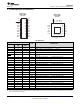
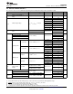
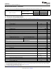
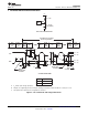
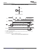
5 Pin Configuration and Functions
PW Package
24-Pin TSSOP
Top View
RGE Package
24-Pin VQFN
Top View
(1) V
DPUX
is the pull-up reference voltage for the associated data line. V
DPUM
is the master I
2
C reference voltage and V
DPU0
-V
DPU7
are the
slave channel reference voltages.
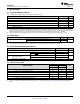
Pin Functions
PIN
TYPE DESCRIPTION
NAME
TSSOP
(PW)
QFN
(RGE)
A0 1 22 I Address input 0. Connect directly to V
CC
or ground
A1 2 23 I Address input 1. Connect directly to V
CC
or ground
A2 21 18 I Address input 2. Connect directly to V
CC
or ground
GND 12 9 — Ground
RESET 3 24 I
Active-low reset input. Connect to V
CC
or V
DPUM
(1)
through a pull-up resistor, if
not used
SD0 4 1 I/O Serial data 0. Connect to V
DPU0
(1)
through a pull-up resistor
SC0 5 2 I/O Serial clock 0. Connect to V
DPU0
(1)
through a pull-up resistor
SD1 6 3 I/O Serial data 1. Connect to V
DPU1
(1)
through a pull-up resistor
SC1 7 4 I/O Serial clock 1. Connect to V
DPU1
(1)
through a pull-up resistor
SD2 8 5 I/O Serial data 2. Connect to V
DPU2
(1)
through a pull-up resistor
SC2 9 6 I/O Serial clock 2. Connect to V
DPU2
(1)
through a pull-up resistor
SD3 10 7 I/O Serial data 3. Connect to V
DPU3
(1)
through a pull-up resistor
SC3 11 8 I/O Serial clock 3. Connect to V
DPU3
(1)
through a pull-up resistor
SD4 13 10 I/O Serial data 4. Connect to V
DPU4
(1)
through a pull-up resistor
SC4 14 11 I/O Serial clock 4. Connect to V
DPU4
(1)
through a pull-up resistor
SD5 15 12 I/O Serial data 5. Connect to V
DPU5
(1)
through a pull-up resistor
SC5 16 13 I/O Serial clock 5. Connect to V
DPU5
(1)
through a pull-up resistor
SD6 17 14 I/O Serial data 6. Connect to V
DPU6
(1)
through a pull-up resistor
SC6 18 15 I/O Serial clock 6. Connect to V
DPU6
(1)
through a pull-up resistor
SD7 19 16 I/O Serial data 7. Connect to V
DPU7
(1)
through a pull-up resistor
SC7 20 17 I/O Serial clock 7. Connect to V
DPU7
(1)
through a pull-up resistor
SCL 22 19 I/O Serial clock bus. Connect to V
DPUM
(1)
through a pull-up resistor
SDA 23 20 I/O Serial data bus. Connect to V
DPUM
(1)
through a pull-up resistor
VCC 24 21 Power Supply voltage