
SP3485 datasheet
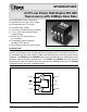

10/15/02 SP3481/3485 Low Power Half-Duplex RS485 Transceivers © Copyright 2000 Sipex Corporation
2
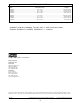
SPECIFICATIONS
T
AMB
= T
MIN
to T
MAX
and V
CC
= +3.3V ± 5% unless otherwise noted.
PARAMETERS MIN. TYP. MAX. UNITS CONDITIONS
SP3481/SP3485 DRIVER
DC Characteristics
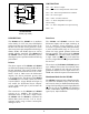
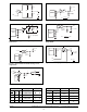
Differential Output Voltage GND V
CC
Volts Unloaded; R = ∞;
Figure 1
Differential Output Voltage 2 V
CC
Volts with load; R = 50Ω; (RS-422);
Figure 1
Differential Output Voltage 1.5 V
CC
Volts with load; R = 27Ω; (RS-485);
Figure 1
Change in Magnitude of Driver
Differential Output Voltage for
Complimentary States 0.2 Volts R = 27Ω or R = 50Ω;
Figure 1
Driver Common-Mode
Output Voltage 3 Volts R = 27Ω or R = 50Ω;
Figure 1
Input High Voltage 2.0 Volts Applies to DE, DI, RE
Input Low Voltage 0.8 Volts Applies to DE, DI, RE
Input Current ±10 µA Applies to DE, DI, RE
Driver Short-Circuit Current
V
OUT
= HIGH ±250 mA -7V ≤ V
O
≤ +12V
V
OUT
= LOW ±250 mA -7V ≤ V
O
≤ +12V
SP3481/SP3485 DRIVER
AC Characteristics
Maximum Data Rate 10 Mbps RE = V
CC
, DE = V
CC
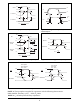
Driver Input to Output, t
PLH
20 40 60 ns
Figures 2 and 8
Driver Input to Output, t
PHL
20 40 60 ns
Figures 2 and 8
Differential Driver Skew 2 10 ns t
DO1
- t
DO2
Figures 2 and 9
Driver Rise or Fall Time 5 20 ns From 10% to 90% ;
Figures 3 and
9
Driver Enable to Output High 52 120 ns
Figures 4 and 10
Driver Enable to Output Low 60 120 ns
Figures 5 and 10
Driver Disable Time from Low 40 120 ns
Figures 5 and 10
Driver Disable Time from High 60 120 ns
Figures 4 and 10
SP3481/SP3485
RECEIVER
DC Characteristics
Differential Input Threshold -0.2 +0.2 Volts -7V ≤ V
CM
≤ +12V
Input Hysteresis 20 mV V
CM
= 0V
Output Voltage High V
CC
-0.4 Volts V
ID
= +200mV, -1.5mA
Output Voltage Low 0.4 Volts V
ID
= -200mV, 2.5mA
Three-State (High Impedance)
Output Current +1 µA 0V ≤ V
O
≤ V
CC
; RE = V
CC
Input Resistance 12 15 kΩ -7V ≤ V
CM
≤ +12V
Input Current (A, B); V
IN
= 12V 1.0 mA DE = 0V, V
CC
= 0V or 3.6V, V
IN
= 12V
Input Current (A, B); V
IN
= -7V -0.8 mA DE = 0V, V
CC
= 0V or 3.6V, V
IN
= -7V
Short-Circuit Current 7 60 mA 0V ≤ V
CM
≤ V
CC
ABSOLUTE MAXIMUM RATINGS
These are stress ratings only and functional operation of the device at
these ratings or any other above those indicated in the operation sections
of the specifications below is not implied. Exposure to absolute maximum
rating conditions for extended periods of time may affect reliability.
V
CC
............................................................................................. +6.0V
Input Voltages
Logic ..................................................... -0.3V to +6.0V
Drivers ................................................... -0.3V to +6.0V
Receivers ............................................................ ±15V
Output Voltages
Drivers .................................................................. ±15V
Receivers .............................................. -0.3V to +6.0V
Storage Temperature ................................................ .-65˚C to +150˚C
Power Dissipation per Package
8-pin NSOIC (derate 6.90mW/
o
C above +70
o
C) ..................... 600mW
8-pin PDIP (derate 11.8mW/
o
C above +70
o
C) ...................... 1000mW