
Data Sheet

992
Atmel | SMART SAM D21 [DATASHEET]
Atmel-42181G–SAM-D21_Datasheet–09/2015
36.14.4 SWD Timing
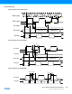
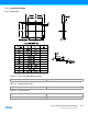
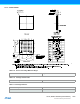
Figure 36-23.SWD Interface Signals
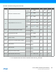
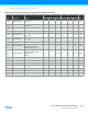
Table 36-62. SWD Timings
(1)
Note: 1. These values are based on simulation. These values are not covered by test limits in production or
characterization.
Symbol Parameter Conditions Min. Max. Units
Thigh SWDCLK High period
V
VDDIO
from 3.0V to 3.6V,
maximum external capacitor =
40pF
10 500000
ns
Tlow SWDCLK Low period 10 500000
Tos
SWDIO output skew to falling edge
SWDCLK
-5 5
Tis
Input Setup time required between
SWDIO
4 -
Tih
Input Hold time required between
SWDIO and rising edge SWDCLK
1 -
Stop Park Tri State
AcknowledgeTri State Tri State
Parity Sta
rt
Data Data
Stop Park Tri State
AcknowledgeTri State
Sta
rt
Read Cycle
W
rite Cycle
Tos
Thigh
Tlow
Tis
Data Data Parity Tri State
Tih
Fro
m debugger to
SWDIO pin
Fro
m debugger to
S
WDCLK pin
S
WDIO pin to
debugger
Fro
m debugger to
SWDIO pin
Fro
m debugger to
S
WDCLK pin
S
WDIO pin to
debugger