
Data Sheet

964
Atmel | SMART SAM D21 [DATASHEET]
Atmel-42181G–SAM-D21_Datasheet–09/2015
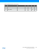
Notes: 1. According to the standard equation V(X)=V
LSB
*(X+1); V
LSB
=V
DDANA
/64
2. Data computed with the Best Fit method
3. Data computed using histogram
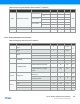
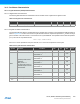
36.9.7 Internal 1.1V Bandgap Reference Characteristics
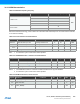
Table 36-35. Bandgap and Internal 1.1V reference characteristics
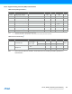
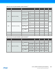
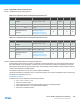
Table 36-34. Electrical and Timing, Device Variant B
Symbol Parameter Conditions Min. Typ. Max. Units
I
Positive input voltage
range
I
0 - V
DDANA
V
I
Negative input voltage
range
I
0 - V
DDANA
I
Offset
Hysteresis = 0, Fast mode -15 0.0 +15 mV
Hysteresis = 0, Low power mode -25 0.0 +25 mV
Hysteresis
Hysteresis = 1, Fast mode 20 50 85 mV
Hysteresis = 1, Low power mode 15 40 75 mV
Propagation delay
Changes for V
ACM
=V
DDANA
/2
100mV overdrive, Fast mode
- 90 180 ns
Changes for V
ACM
=V
DDANA
/2
100mV overdrive, Low power
mode
- 282 520 ns
t
STARTUP
Startup time
Enable to ready delay
Fast mode
- 1 2.6 µs
Enable to ready delay
Low power mode
- 14 22 µs
V
SCALE
INL
(3)
-1.4 0.75 +1.4 LSB
DNL
(3)
-0.9 0.25 +0.9 LSB
Offset Error
(1)(2)
-0.200 0.260 +0.920 LSB
Gain Error
(1)(2)
-0.89 0.215 0.89 LSB
Symbol Parameter Conditions Min. Typ. Max. Units
INT1V
Internal 1.1V Bandgap
reference
After calibration at T= 25°C,
over [-40, +85]C
1.08 1.1 1.12 V
Over voltage at 25°C 1.09 1.1 1.11 V