
Data Sheet


96
Atmel | SMART SAM D21 [DATASHEET]
Atmel-42181G–SAM-D21_Datasheet–09/2015
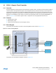
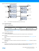
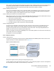
Figure 14-2. Generic Clock Controller Block Diagram
(1)
Note: 1. If the GENCTRL.SRC=GCLKIN the GCLK_IO is set as an input.
14.4 Signal Description
Refer to “I/O Multiplexing and Considerations” on page 21 for details on the pin mapping for this peripheral. One signal
can be mapped on several pins.
14.5 Product Dependencies
In order to use this peripheral, other parts of the system must be configured correctly, as described below.
14.5.1 I/O Lines
Using the Generic Clock Controller’s I/O lines requires the I/O pins to be configured. Refer to “PORT” on page 379 for
details.
14.5.2 Power Management
The Generic Clock Controller can operate in all sleep modes, if required. Refer to Table 15-4 for details on the different
sleep modes.
14.5.3 Clocks
The Generic Clock Controller bus clock (CLK_GCLK_APB) can be enabled and disabled in the Power Manager, and the
default state of CLK_GCLK_APB can be found in the Peripheral Clock Masking section in APBAMASK.
Generic Clock Generator 0
GC
LK_I
O
[0]
(
I/O input)
C
lock
D
ivider
&
Maske
r
C
lock
S
ources
GCLKGEN
[
0
]
GC
LK_I
O
[1]
(
I/O input
)
GC
LK
G
EN[1]
G
CLK
_
IO
[
n
]
(
I
/O
input
)
GC
LK
G
EN[n]
Clock
G
at
e
G
eneric
C
lock Multiplexer
0
GCLK_PERIPHERAL[0]
Clock
G
at
e
G
eneric
C
lock Multiplexer 1
C
lock
G
at
e
G
eneric Clock Multi
p
lexer
m
GC
LK
G
EN[n:0]
GC
LK_MAIN
GC
LK_I
O
[1
]
(
I
/O
output
)
GC
LK_I
O
[0
]
(I/O output
)
GCLK
_
IO
[
n
]
(
I
/O
output
)
G
eneric
C
lock
G
enerator
1
C
lock
Divider &
Maske
r
G
eneric
C
lock
G
enerator
n
C
lock
D
ivider
&
M
as
k
er
GCLK_PERIPHERAL[1]
GCLK_PERIPHERAL[m]
Table 14-1. Signal Description
Signal Name Type Description
GCLK_IO[7:0] Digital I/O
Source clock when input
Generic clock when output