
Data Sheet

957
Atmel | SMART SAM D21 [DATASHEET]
Atmel-42181G–SAM-D21_Datasheet–09/2015
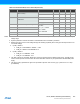
Notes: 1. Maximum numbers are based on characterization and not tested in production, and valid for 5% to 95% of the input
voltage range.
2. Dynamic parameter numbers are based on characterization and not tested in production.
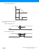
3. Respect the input common mode voltage through the following equations (where VCM_IN is the Input channel com-
mon mode voltage):
a. If |VIN| > VREF/4
z VCM_IN < 0.95*VDDANA + VREF/4 – 0.75V
z VCM_IN > VREF/4 -0.05*VDDANA -0.1V
b. If |VIN| < VREF/4
z VCM_IN < 1.2*VDDANA - 0.75V
z VCM_IN > 0.2*VDDANA - 0.1V
4. The ADC channels on pins PA08, PA09, PA10, PA11 are powered from the VDDIO power supply. The ADC perfor-
mance of these pins will not be the same as all the other ADC channels on pins powered from the VDDANA power
supply.
5. The gain accuracy represents the gain error expressed in percent. Gain accuracy (%) = (Gain Error in V x 100) /
(2*Vref/GAIN)
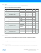
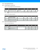
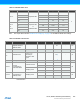
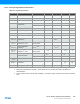
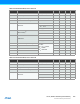
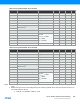
Gain Accuracy
(5)
Ext. Ref. 0.5x +/-0.02 +/-0.05 +/-0.1 %
Ext. Ref. 2x to 16x +/-0.01 +/-0.03 +/-0.5 %
Offset Error
Ext. Ref. 1x -5.0 -1.0 +5.0 mV
V
REF
=V
DDANA
/1.48 -5.0 -0.6 +5.0 mV
Bandgap -5.0 -1.0 +5.0 mV
SFDR Spurious Free Dynamic Range
1x Gain
F
CLK_ADC
= 2.1MHz
F
IN
= 40kHz
A
IN
= 95%FSR
65 71.3 77.0 dB
SINAD Signal-to-Noise and Distortion 58 65 67 dB
SNR Signal-to-Noise Ratio 60 66 68.6 dB
THD Total Harmonic Distortion -75 -71 -67.0 dB
Noise RMS T=25°C 0.6 1.0 1.6 mV
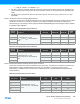
Table 36-23. Differential Mode, Device Variant B (Continued)
Symbol Parameter Conditions Min. Typ. Max. Units