
Data Sheet


91
Atmel | SMART SAM D21 [DATASHEET]
Atmel-42181G–SAM-D21_Datasheet–09/2015
CTRL.SWRST bit has no effect. The Synchronisation Ready interrupt (if available) cannot be used for Software Reset
write-synchronization.
When the software reset is in progress (STATUS.SYNCBUSY and CTRL.SWRST are one), attempt to do any of the
following will cause the peripheral bus to stall until the Software Reset synchronization and the reset is complete:
z Writing a core register
z Writing an APB register
z Reading a read-synchronized register
APB registers can be read while the software reset is being write-synchronized without causing the peripheral bus to
stall.
13.3.1.8 Synchronization Delay
The synchronization will delay the write or read access duration by a delay D, given by the equation:
Where is the period of the generic clock and is the period of the peripheral bus clock. A normal peripheral
bus register access duration is .
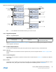
13.3.2 Distributed Synchronizer Register Synchronization
13.3.2.1 Overview
All peripherals are composed of one digital bus interface, which is connected to the APB or AHB bus and clocked using a
corresponding synchronous clock, and one core clock, which is clocked using a generic clock. Access between these
clock domains must be synchronized. As this mechanism is implemented in hardware the synchronization process takes
place even if the different clocks domains are clocked from the same source and on the same frequency. All registers in
the bus interface are accessible without synchronization. All core registers in the generic clock domain must be
synchronized when written. Some core registers must be synchronized when read. Registers that need synchronization
has this denoted in each individual register description.
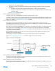
13.3.2.2 General Write synchronization
Inside the same module, each core register, denoted by the Write-Synchronized property, use its own synchronization
mechanism so that writing to different core registers can be done without waiting for the end of synchronization of
previous core register access.
To write again to the same core register in the same module, user must wait for the end of synchronization or the write
will be discarded.
For each core register, that can be written, a synchronization status bit is associated
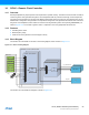
Example:
REGA, REGB are 8-bit core registers. REGC is 16-bit core register.
Since synchronization is per register, user can write REGA (8-bit access) then immediately write REGB (8-bit access)
without error.
User can write REGC (16-bit access) without affecting REGA or REGB. But if user writes REGC in two consecutives 8-bit
accesses, second write will be discarded and generate an error.
5 P
GCLK
⋅ 2 P
APB
⋅+ D 6 P
GCLK
⋅ 3 P
APB
⋅+<<
P
GCLK
P
APB
2 P
APB
⋅
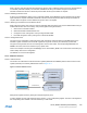
Offset Register
0x00 REGA
0x01 REGB
0x02
REGC
0x03