
Data Sheet

869
Atmel | SMART SAM D21 [DATASHEET]
Atmel-42181G–SAM-D21_Datasheet–09/2015
z Bits 23:20 – INPUTOFFSET[3:0]: Positive Mux Setting Offset
The pin scan is enabled when INPUTSCAN != 0. Writing these bits to a value other than zero causes the first con-
version triggered to be converted using a positive input equal to MUXPOS + INPUTOFFSET. Setting this register
to zero causes the first conversion to use a positive input equal to MUXPOS.
After a conversion, the INPUTOFFSET register will be incremented by one, causing the next conversion to be
done with the positive input equal to MUXPOS + INPUTOFFSET. The sum of MUXPOS and INPUTOFFSET gives
the input that is actually converted.
z Bits 19:16 – INPUTSCAN[3:0]: Number of Input Channels Included in Scan
This register gives the number of input sources included in the pin scan. The number of input sources included is
INPUTSCAN + 1. The input channels included are in the range from MUXPOS + INPUTOFFSET to MUXPOS +
INPUTOFFSET + INPUTSCAN.
The range of the scan mode must not exceed the number of input channels available on the device.
z Bits 15:13 – Reserved
These bits are unused and reserved for future use. For compatibility with future devices, always write these bits to
zero when this register is written. These bits will always return zero when read.
z Bits 12:8 – MUXNEG[4:0]: Negative Mux Input Selection
These bits define the Mux selection for the negative ADC input. Table 32-13 shows the possible input selections.
0x4 16X 16x
0x5-0xE Reserved
0xF DIV2 1/2x
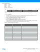
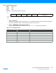
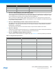
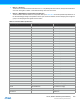
Table 32-13. Negative Mux Input Selection
Value Name Description
0x00 PIN0 ADC AIN0 pin
0x01 PIN1 ADC AIN1 pin
0x02 PIN2 ADC AIN2 pin
0x03 PIN3 ADC AIN3 pin
0x04 PIN4 ADC AIN4 pin
0x05 PIN5 ADC AIN5 pin
0x06 PIN6 ADC AIN6 pin
0x07 PIN7 ADC AIN7 pin
0x08-0x17 – Reserved
0x18 GND Internal ground
0x19 IOGND I/O ground
0x1A-0x1F – Reserved
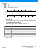
GAIN[3:0] Name Description