
Data Sheet

865
Atmel | SMART SAM D21 [DATASHEET]
Atmel-42181G–SAM-D21_Datasheet–09/2015
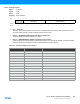
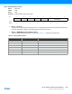
Table 32-10. Conversion Result Resolution
z Bit 3 – CORREN: Digital Correction Logic Enabled
0: Disable the digital result correction.
1: Enable the digital result correction. The ADC conversion result in the RESULT register is then corrected for gain
and offset based on the values in the GAINCAL and OFFSETCAL registers. Conversion time will be increased by
X cycles according to the value in the Offset Correction Value bit group in the Offset Correction register.
z Bit 2 – FREERUN: Free Running Mode
0: The ADC run is single conversion mode.
1: The ADC is in free running mode and a new conversion will be initiated when a previous conversion completes.
z Bit 1 – LEFTADJ: Left-Adjusted Result
0: The ADC conversion result is right-adjusted in the RESULT register.
1: The ADC conversion result is left-adjusted in the RESULT register. The high byte of the 12-bit result will be
present in the upper part of the result register. Writing this bit to zero (default) will right-adjust the value in the
RESULT register.
z Bit 0 – DIFFMODE: Differential Mode
0: The ADC is running in singled-ended mode.
1: The ADC is running in differential mode. In this mode, the voltage difference between the MUXPOS and MUX-
NEG inputs will be converted by the ADC.
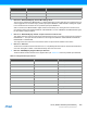
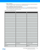
RESSEL[1:0] Name Description
0x0 12BIT 12-bit result
0x1 16BIT For averaging mode output
0x2 10BIT 10-bit result
0x3 8BIT 8-bit result