
Data Sheet

845
Atmel | SMART SAM D21 [DATASHEET]
Atmel-42181G–SAM-D21_Datasheet–09/2015
z Event-triggered conversion for accurate timing (one event input)
z Optional DMA transfer of conversion result
z Hardware gain and offset compensation
z Averaging and oversampling with decimation to support, up to 16-bit result
z Selectable sampling time
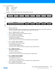
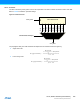
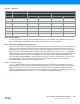
32.3 Block Diagram
Figure 32-1. ADC Block Diagram
32.4 Signal Description
Note: 1. Refer to “Configuration Summary” on page 3 for details on exact number of analog input channels.
Refer to “I/O Multiplexing and Considerations” on page 21 for details on the pin mapping for this peripheral. One signal
can be mapped on several pins.
ADC
ADC0
ADCn
...
INT.SIG
ADC0
ADCn
INT.SIG
...
REFCTRL
INT1V
INTVCC
VREFB
OFFSETCORR
GAINCORRSWTRIG
EVCTRL
AVGCTRL
WINCTRL
SAMPCTRL WINUT
POST
PROCESSING
PRESCALER
CTRLA
WINLT
VREFA
CTRLB
RESULT
INPUTCTRL
Signal Name Type Description
VREFA Analog input External reference voltage A
VREFB Analog input External reference voltage B
ADC[19..0]
(1)
Analog input Analog input channels