
Data Sheet

745
Atmel | SMART SAM D21 [DATASHEET]
Atmel-42181G–SAM-D21_Datasheet–09/2015
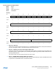
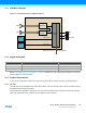
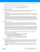
31.3 USB Block Diagram
Figure 31-1. LS/FS Implementation: USB Block Diagram
31.4 Signal Description
Refer to “I/O Multiplexing and Considerations” on page 21 for details on the pin mapping for this peripheral. One signal
can be mapped to one of several pins.
31.5 Product Dependencies
In order to use this peripheral module, other parts of the system must be configured correctly, as described below.
31.5.1 I/O Lines
The USB pins may be multiplexed with the I/O lines Controller. The user must first configure the I/O Controller to assign
the USB pins to their peripheral functions.
A 1kHz SOF clock is available on external pin. The user must first configure the I/O Controller to assign the 1kHz SOF
clock to the peripheral function. The SOF clock is available for device and host.
User
interface
AHB Master
USB 2.0
Core
USB
AHB
APB
NVIC
GCLK
USB interrupts
GCLK_USB
System clock domain USB clock domain
DM
DP
SOF 1kHz
Pin Name Pin Description Type
DM Data -: Differential Data Line - Port Input/Output
DP Data +: Differential Data Line + Port Input/Output
SOF 1kHZ SOF Output Output