
Data Sheet

678
Atmel | SMART SAM D21 [DATASHEET]
Atmel-42181G–SAM-D21_Datasheet–09/2015
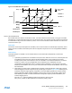
30.6.3.7 Waveform Extension
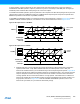
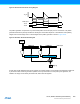
Figure 30-33 shows a schematic diagram of action of the four optional units following the recoverable fault stage, on a
port pin pair. The DTI and SWAP units can be seen as a four port pair slices:
z Slice 0 DTI0 / SWAP0 acting on port pins (WO[0], WO[WO_NUM/2 +0])
z Slice 1 DTI1 / SWAP1 acting on port pins (WO[1], WO[WO_NUM/2 +1])
And more generally:
z Slice n DTIx / SWAPx acting on port pins (WO[x], WO[WO_NUM/2 +x])
Figure 30-33.Waveform Extension Stage Details
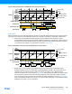
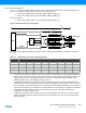
The output matrix (OTMX) unit distributes compare channels, according to the selectable configurations, as shown in
Table 30-3.
z Configuration 0x0 is default configuration. The channel location is the default one and channels are distributed on
outputs modulo the number of channels. Channel 0 is routed to the Output matrix output OTMX[0], Channel 1 to
OTMX[1]. If there are more outputs than channels, then channel 0 is duplicated to the Output matrix output
OTMX[CC_NUM], channel 1 to OTMX[CC_NUM+1] and so on.
z Configuration 0x1 distributes the channels on output modulo half the number of channels, this gives the lower
channels twice the number of output locations than the default configuration. This provides for example, control of
the four transistors of a full bridge using only two compare channels. Using pattern generation, some of these four
outputs can be overwritten by a constant level, enabling flexible drive of a full bridge in all quadrant configurations.
z Configuration 0x2 distributes the compare channel 0 (CC0) to all port pins. With pattern generation, this
configuration can control a stepper motor.
z Configuration 0x3 distributes the compare channel CC0 to first output and the channel CC1 to all other outputs.
Together with pattern generation and the fault extension this configuration can control up to seven LED strings,
with a boost stage.
Table 30-3. Output Matrix Channel Pin Routing Configuration
Value OTMX[x]
0x0 CC3 CC2 CC1 CC0 CC3 CC2 CC1 CC0
0x1 CC1 CC0 CC1 CC0 CC1 CC0 CC1 CC0
0x2 CC0 CC0 CC0 CC0 CC0 CC0 CC0 CC0
0x3 CC1 CC1 CC1 CC1 CC1 CC1 CC1 CC0
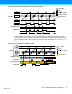
OTMX[x]
DTIx
LS
HS
OTMX[x+WO_NUM/2]
DTIxEN SWAPx
PGO[x+WO_NUM/2]
PGO[x]
PGV[x+WO_NUM/2]
PGV[x]
INV[x+WO_NUM/2]
P[x+WO_NUM/2]
INV[x]
P[x]
PORTSWEX
OTMX
OTMX DTI SWAP PATTERN