
Data Sheet

56
Atmel | SMART SAM D21 [DATASHEET]
Atmel-42181G–SAM-D21_Datasheet–09/2015
For more information, refer to the ARM Debug Interface Version 5 Architecture Specification.
12.10.2 DSU Chip Identification Method:
The DSU DID register identifies the device by implementing the following information:
z Processor identification
z Product family identification
z Product series identification
z Device select
12.11 Functional Description
12.11.1 Principle of Operation
The DSU provides memory services such as CRC32 or MBIST that require almost the same interface. Hence, the
Address, Length and Data registers are shared. They must be configured first; then a command can be issued by writing
the Control register. When a command is ongoing, other commands are discarded until the current operation is
completed. Hence, the user must wait for the STATUSA.DONE bit to be set prior to issuing another one.
12.11.2 Basic Operation
12.11.2.1 Initialization
The module is enabled by enabling its clocks. For more details, refer to “Clocks” on page 51. The DSU registers can be
write-protected. Refer to “PAC – Peripheral Access Controller” on page 41.
12.11.2.2 Operation from a debug adapter
Debug adapters should access the DSU registers in the external address range 0x100 – 0x2000. If the device is
protected by the NVMCTRL security bit (refer to “Security Bit” on page 361), accessing the first 0x100 bytes causes the
system to return an error (refer to “Intellectual Property Protection” on page 54).
12.11.2.3 Operation from the CPU
There are no restrictions when accessing DSU registers from the CPU. However, the user should access DSU registers
in the internal address range (0x0 – 0x100) to avoid external security restrictions (refer to “Intellectual Property
Protection” on page 54).
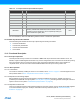
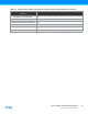
Table 12-2. Conceptual 64-Bit Peripheral ID Bit Descriptions
Field Size Description Location
JEP-106 CC code 4 Atmel continuation code: 0x0 PID4
JEP-106 ID code 7 Atmel device ID: 0x1F PID1+PID2
4KB count 4 Indicates that the CoreSight component is a ROM: 0x0 PID4
RevAnd 4 Not used; read as 0 PID3
CUSMOD 4 Not used; read as 0 PID3
PARTNUM 12 Contains 0xCD0 to indicate that DSU is present PID0+PID1
REVISION 4
DSU revision (starts at 0x0 and increments by 1 at both major and minor
revisions). Identifies DSU identification method variants. If 0x0, this
indicates that device identification can be completed by reading the
Device Identification register (DID)
PID3