
Data Sheet

53
Atmel | SMART SAM D21 [DATASHEET]
Atmel-42181G–SAM-D21_Datasheet–09/2015
reset or external reset occurs. Availability of the Hot-Plugging feature can be read from the Hot-Plugging Enable bit of the
Status B register (STATUSB.HPE).
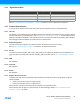
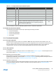
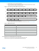
Figure 12-3. Hot-Plugging Detection Timing Diagram
The presence of a debugger probe is detected when either Hot-Plugging or Cold-Plugging is detected. Once detected,
the Debugger Present bit of the Status B register (STATUSB.DBGPRES) is set. For security reasons, Hot-Plugging is not
available when the device is protected by the NVMCTRL security bit (refer to “Security Bit” on page 361).
This detection requires that pads are correctly powered. Thus, at cold startup, this detection cannot be done until POR is
released. If the device is protected, Cold-Plugging is the only way to detect a debugger probe, and so the external reset
timing must be longer than the POR timing. If external reset is deasserted before POR release, the user must retry the
procedure above until it gets connected to the device.
12.7 Chip-Erase
Chip-Erase consists of removing all sensitive information stored in the chip and clearing the NVMCTRL security bit (refer
to “Security Bit” on page 361). Hence, all volatile memories and the flash array (including the EEPROM emulation area)
will be erased. The flash auxiliary rows, including the user row, will not be erased. When the device is protected, the
debugger must reset the device in order to be detected. This ensures that internal registers are reset after the protected
state is removed. The Chip-Erase operation is triggered by writing a one to the Chip-Erase bit in the Control register
(CTRL.CE). This command will be discarded if the DSU is protected by the Peripheral Access Controller (PAC). Once
issued, the module clears volatile memories prior to erasing the flash array. To ensure that the Chip-Erase operation is
completed, check the Done bit of the Status A register (STATUSA.DONE). The Chip-Erase operation depends on clocks
and power management features that can be altered by the CPU. For that reason, it is recommended to issue a Chip-
Erase after a Cold-Plugging procedure to ensure that the device is in a known and safe state.
The recommended sequence is as follows:
1. Issue the Cold-Plugging procedure (refer to “Cold-Plugging” on page 52). The device then:
1. Detects the debugger probe
2. Holds the CPU in reset
2. Issue the Chip-Erase command by writing a one to CTRL.CE. The device then:
1. Clears the system volatile memories
2. Erases the whole flash array (including the EEPROM emulation area, not including auxiliary rows)
3. Erases the lock row, removing the NVMCTRL security bit protection
3. Check for completion by polling STATUSA.DONE (read as one when completed).
4. Reset the device to let the NVMCTRL update fuses.
12.8 Programming
Programming of the flash or RAM memories is available when the device is not protected by the NVMCTRL security bit
(refer to “Security Bit” on page 361).
SWCLK
Hot-Plugging
CPU_STATE
reset
running
R
ESET