
Data Sheet

493
Atmel | SMART SAM D21 [DATASHEET]
Atmel-42181G–SAM-D21_Datasheet–09/2015
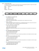
0: The data is sampled on a leading SCK edge and changed on a trailing SCK edge.
1: The data is sampled on a trailing SCK edge and changed on a leading SCK edge.
This bit is not synchronized.
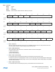
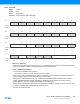
Table 26-4. SPI Transfer Modes
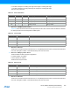
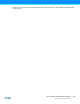
z Bits 27:24 – FORM[3:0]: Frame Format
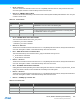
Table 26-5 shows the various frame formats supported by the SPI. When a frame format with address is selected,
the first byte received is checked against the ADDR register.
Table 26-5. Frame Format
z Bits 23:22 – Reserved
These bits are unused and reserved for future use. For compatibility with future devices, always write these bits to
zero when this register is written. These bits will always return zero when read.
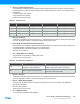
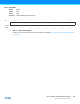
z Bits 21:20 – DIPO[1:0]: Data In Pinout
These bits define the data in (DI) pad configurations.
In master operation, DI is MISO.
In slave operation, DI is MOSI.
These bits are not synchronized.
Table 26-6. Data In Pinout
z Bits 19:18 – Reserved
These bits are unused and reserved for future use. For compatibility with future devices, always write these bits to
zero when this register is written. These bits will always return zero when read.
Mode CPOL CPHA Leading Edge Trailing Edge
0x0 0 0 Rising, sample Falling, change
0x1 0 1 Rising, change Falling, sample
0x2 1 0 Falling, sample Rising, change
0x3 1 1 Falling, change Rising, sample
FORM[3:0] Name Description
0x0 SPI SPI frame
0x1 - Reserved
0x2 SPI_ADDR SPI frame with address
0x3-0xF - Reserved
DIPO[1:0] Name Description
0x0 PAD[0] SERCOM PAD[0] is used as data input
0x1 PAD[1] SERCOM PAD[1] is used as data input
0x2 PAD[2] SERCOM PAD[2] is used as data input
0x3 PAD[3] SERCOM PAD[3] is used as data input