
Data Sheet

492
Atmel | SMART SAM D21 [DATASHEET]
Atmel-42181G–SAM-D21_Datasheet–09/2015
26.8.1 Control A
Name: CTRLA
Offset: 0x00
Reset: 0x00000000
Property: Write-Protected, Enable-Protected, Write-Synchronized
z Bit 31 – Reserved
This bit is unused and reserved for future use. For compatibility with future devices, always write this bit to zero
when this register is written. This bit will always return zero when read.
z Bit 30 – DORD: Data Order
This bit indicates the data order when a character is shifted out from the Data register.
0: MSB is transferred first.
1: LSB is transferred first.
This bit is not synchronized.
z Bit 29 – CPOL: Clock Polarity
In combination with the Clock Phase bit (CPHA), this bit determines the SPI transfer mode.
0: SCK is low when idle. The leading edge of a clock cycle is a rising edge, while the trailing edge is a falling edge.
1: SCK is high when idle. The leading edge of a clock cycle is a falling edge, while the trailing edge is a rising edge.
This bit is not synchronized.
z Bit 28 – CPHA: Clock Phase
In combination with the Clock Polarity bit (CPOL), this bit determines the SPI transfer mode.
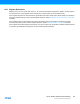
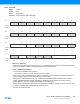
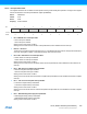
Bit3130292827262524
DORD CPOL CPHA FORM[3:0]
Access R R/W R/W R/W R/W R/W R/W R/W
Reset00000000
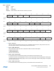
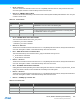
Bit2322212019181716
DIPO[1:0] DOPO[1:0]
Access R R R/W R/W R R R/W R/W
Reset00000000
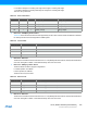
Bit151413121110 9 8
IBON
AccessRRRRRRRR/W
Reset00000000
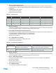
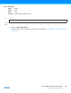
Bit76543210
RUNSTDBY
MODE[2:0] ENABLE SWRST
Access R/W R R R/W R/W R/W R/W R/W
Reset00000000