
Data Sheet

387
Atmel | SMART SAM D21 [DATASHEET]
Atmel-42181G–SAM-D21_Datasheet–09/2015
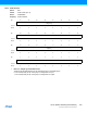
22.7 Register Summary
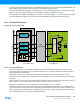
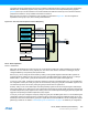
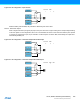
The I/O pins are organized in groups with up to 32 pins. Group 0 consists of the PA pins, group 1 the PB pins, etc. Each
group has its own set of registers. For example, the register address offset for the Data Direction (DIR) register for group
0 (PA00 to PA31) is 0x00, while the register address offset for the DIR register for group 1 (PB00 to PB31) is 0x80.
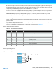
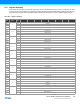
Table 22-2. Register Summary
Offset Name
Bit
Pos.
0x00
DIR
7:0 DIR[7:0]
0x01 15:8 DIR[15:8]
0x02 23:16 DIR[23:16]
0x03 31:24 DIR[31:24]
0x04
DIRCLR
7:0 DIRCLR[7:0]
0x05 15:8 DIRCLR[15:8]
0x06 23:16 DIRCLR[23:16]
0x07 31:24 DIRCLR[31:24]
0x08
DIRSET
7:0 DIRSET[7:0]
0x09 15:8 DIRSET[15:8]
0x0A 23:16 DIRSET[23:16]
0x0B 31:24 DIRSET[31:24]
0x0C
DIRTGL
7:0 DIRTGL[7:0]
0x0D 15:8 DIRTGL[15:8]
0x0E 23:16 DIRTGL[23:16]
0x0F 31:24 DIRTGL[31:24]
0x10
OUT
7:0 OUT[7:0]
0x11 15:8 OUT[15:8]
0x12 23:16 OUT[23:16]
0x13 31:24 OUT[31:24]
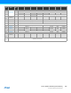
0x14
OUTCLR
7:0 OUTCLR[7:0]
0x15 15:8 OUTCLR[15:8]
0x16 23:16 OUTCLR[23:16]
0x17 31:24 OUTCLR[31:24]
0x18
OUTSET
7:0 OUTSET[7:0]
0x19 15:8 OUTSET[15:8]
0x1A 23:16 OUTSET[23:16]
0x1B 31:24 OUTSET[31:24]
0x1C
OUTTGL
7:0 OUTTGL[7:0]
0x1D 15:8 OUTTGL[15:8]
0x1E 23:16 OUTTGL[23:16]
0x1F 31:24 OUTTGL[31:24]
0x20
IN
7:0 IN[7:0]
0x21 15:8 IN[15:8]
0x22 23:16 IN[23:16]
0x23 31:24 IN[31:24]
0x24
CTRL
7:0 SAMPLING[7:0]
0x25 15:8 SAMPLING[15:8]
0x26 23:16 SAMPLING[23:16]
0x27 31:24 SAMPLING[31:24]