
Data Sheet

384
Atmel | SMART SAM D21 [DATASHEET]
Atmel-42181G–SAM-D21_Datasheet–09/2015
By default, the input synchronizer is clocked only when an input read is requested, which will delay the read operation by
two CLK_PORT cycles. To remove that delay, the input synchronizers for each group of eight pins can be configured to
be always active, but this comes at the expense of higher power consumption. This is controlled by writing a one to the
corresponding SAMPLINGn bit group of the CTRL register, where n = (y%32) / 8.
To use pin y as one of the available peripheral functions for that pin, configure it by writing a one to the corresponding
PMUXEN bit of the PINCFGy register. The PINCFGy register for pin y is at byte offset (PINCFG0 + (y%32)).
The peripheral function can be selected by writing to the PMUXO or PMUXE bit group in the PMUXn register. The
PMUXO/PMUXE bit group is at byte offset (PMUX0 + (y%32) / 2), in bits 3:0 if y is even and in bits 7:4 if y is odd.
The chosen peripheral must also be configured and enabled.
22.6.3 I/O Pin Configuration
The Pin Configuration register (PINCFGy) is used for additional I/O pin configuration. A pin can be set in a totem-pole or
pull configuration.
Because pull configuration is done through the Pin Configuration register, all intermediate PORT states during switching
of pin direction and pin values are avoided.
The I/O pin configurations are described further in this chapter, and summarized in Table 22-1.
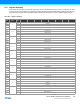
22.6.3.1 Pin Configurations Summary
Table 22-1. Pin Configurations Summary
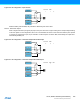
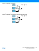
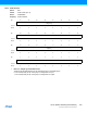
22.6.3.2 Input Configuration
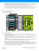
Figure 22-4. I/O Configuration - Standard Input
DIR INEN PULLEN OUT Configuration
0 0 0 X Reset or analog I/O; all digital disabled
0 0 1 0 Pull-down; input disabled
0 0 1 1 Pull-up; input disabled
0 1 0 X Input
0 1 1 0 Input with pull-down
0 1 1 1 Input with pull-up
1 0 X X Output; input disabled
1 1 X X Output; input enabled
PULLEN
DIR
OU
T
IN
INEN
PULLEN
I
NEN
DIR
0
1
0