
Data Sheet

380
Atmel | SMART SAM D21 [DATASHEET]
Atmel-42181G–SAM-D21_Datasheet–09/2015
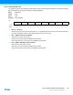
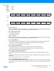
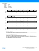
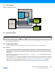
22.3 Block Diagram
Figure 22-1. PORT Block Diagram
22.4 Signal Description
Refer to “I/O Multiplexing and Considerations” on page 21 for details on the pin mapping for this peripheral. One signal
can be mapped on several pins.
22.5 Product Dependencies
In order to use this peripheral, other parts of the system must be configured correctly, as described below.
22.5.1 I/O Lines
The I/O lines of the PORT are mapped to pins of the physical device package according to a simple naming scheme.
Each port group of up to 32 pins is assigned a letter identifier, starting with A, that monotonically increases through the
alphabet for each subsequent port group. Within each port group, each pin is assigned a numerical identifier according to
its bit position.
The resulting PORT pins are mapped as Pxy, where x=A, B, C,… and y=00, 01, …, 31 to uniquely identify each pin in the
device, e.g., PA24, PC03, etc.
Each pin may have one or more peripheral multiplexer settings, which allow the pin to be routed internally to a dedicated
peripheral function. When enabled, the selected peripheral is given control over the output state of the pin, as well as the
ability to read the current physical pin state. Refer to “I/O Multiplexing and Considerations” on page 21 for details.
Device-specific configurations may result in some pins (and the corresponding Pxy pin) not being implemented.
ANALOG
BLOCKS
PERIPHERALS
Digital Controls of Analog Blocks
Analog Pin
Connections
I/O
PINS
Port Line
Interface
IP Line Interface
Peripheral Mux Select
PORT
Control
and
Status
Pin Line
Interface
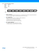
Signal Name Type Description
Pxy Digital I/O General-purpose I/O pin y