
Data Sheet


1082
Atmel | SMART SAM D21 [DATASHEET]
Atmel-42181G–SAM-D21_Datasheet–09/2015
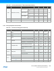
Performance with the hardware offset and gain correction
Inherent gain and offset errors affect the absolute accuracy of the ADC. The offset error cancellation is handled by the
Offset Correction register (OFFSETCORR) and the gain error cancellation, by the Gain Correction register
(GAINCORR). The offset and gain correction value is subtracted from the converted data before writing the Result
register (RESULT).
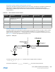
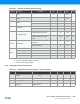
Inputs and Sample and Hold Acquisition Times
The analog voltage source must be able to charge the sample and hold (S/H) capacitor in the ADC in order to achieve
maximum accuracy. Seen externally the ADC input consists of a resistor ( ) and a capacitor ( ). In
addition, the source resistance ( ) must be taken into account when calculating the required sample and hold
time. Figure A-3 shows the ADC input channel equivalent circuit.
Figure A-3. ADC Input
To achieve n bits of accuracy, the capacitor must be charged at least to a voltage of
The minimum sampling time for a given can be found using this formula:
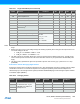
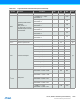
Table A-21. Offset and Gain Correction Feature
Gain Factor Conditions Offset Error (mV) Gain Error (mV)
Total Unadjusted Error
(LSB)
0.5x
In differential mode, 1x gain,
VDDANA=3.0V, VREF=1.0V,
350kSps at 25 C
0.25 1 2.4
1x 0.2 0.1 1.5
2x 0.15 -0.15 2.7
8x -0.05 0.05 3.2
16x 0.1 -0.05 6.1
R
SAMPLE
C
SAMPLE
R
SOURCE
R
SOURCE
R
SAMPLE
Analog Input
AINx
C
SAMPLE
V
IN
VDDANA/2
C
SAMPLE
V
CSAMPLE
V≥
IN
12
n 1+()–
–()×
t
SAMPLEHOLD
R
SOURCE