
Data Sheet

1078
Atmel | SMART SAM D21 [DATASHEET]
Atmel-42181G–SAM-D21_Datasheet–09/2015
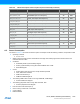
Notes: 1. These values are based on characterization. These values are not covered by test limits in production.
2. These values are based on simulation. These values are not covered by test limits in production or characterization.
3. In this condition and for a sample rate of 350ksps, a conversion takes 6 clock cycles of the ADC clock (conditions: 1X gain, 12-bit resolution, differ-
ential mode, free-running).
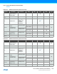
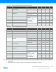
Sampling time
(1)
0.5 - - cycles
Conversion time
(1)
1x Gain 6 - - cycles
V
REF
Voltage reference range 1.0 - V
DDANA
-0.6 V
V
REFINT1V
Internal 1V reference
(2)
- 1.0 - V
V
REFINTVCC0
Internal ratiometric reference 0
(2)
- V
DDANA
/1.48 - V
V
REFINTVCC0
Voltage Error
Internal ratiometric reference 0
(2)
error
2.0V <
V
DDANA
<3.63V
-1.0 - +1.0 %
V
REFINTVCC1
Internal ratiometric reference 1
(2)
V
DDANA
>2.0V - V
DDANA
/2 - V
V
REFINTVCC1
Voltage Error
Internal ratiometric reference 1
(2)
error
2.0V <
V
DDANA
<3.63V
-1.0 - +1.0 %
Conversion range
(1)
Differential mode -V
REF
/GAIN - +V
REF
/GAIN V
Single-ended mode 0.0 - +V
REF
/GAIN V
C
SAMPLE
Sampling capacitance
(2)
- 3.5 - pF
R
SAMPLE
Input channel source resistance
(2)
- - 3.5 kΩ
I
DD
DC supply current
(1)
f
CLK_ADC
= 2.1MHz
I
(3)
- 1.25 1.86 mA
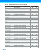
Table A-15. Operating Conditions (Device Variant B) (Continued)
Symbol Parameter Conditions Min. Typ. Max. Units
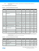
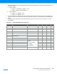
Table A-16. Differential Mode (Device Variant A)
Symbol Parameter Conditions Min. Typ. Max. Units
ENOB Effective Number Of Bits With gain compensation - 10.5 10.9 bits
TUE Total Unadjusted Error
I
1x Gain
n
1.5 4.3 17.0 LSB
INL
I
Integral Non Linearity
1x Gain
n
1.0 1.3 6.5 LSB
DNL Differential Non Linearity
1x Gain
n
+/-0.3 +/-0.5 +/-0.95 LSB
I
I
I
Gain Error
Ext. Ref 1x -15.0 2.5 +20.0 mV
V
REF
=V
DDANA
/1.48 -20 -1.5 +20.0 mV
Bandgap -15.0 -5.0 +15.0 mV