
Data Sheet

1014
Atmel | SMART SAM D21 [DATASHEET]
Atmel-42181G–SAM-D21_Datasheet–09/2015
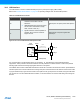
2. Decoupling capacitor should be placed close to the device for each supply pin pair in the signal group.
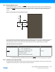
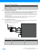
38.6.4 Calculating the Correct Crystal Decoupling Capacitor
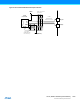
In order to calculate correct load capacitor for a given crystal one can use the model shown in Figure 38-9 which includes
internal capacitors C
Ln
, external parasitic capacitance C
ELn
and external load capacitance C
Pn
.
Figure 38-9. Crystal Circuit With Internal, External and Parasitic Capacitance
Using this model the total capacitive load for the crystal can be calculated as shown in the equation below:
where C
tot
is the total load capacitance seen by the crystal, this value should be equal to the load capacitance value
found in the crystal manufacturer datasheet.
The parasitic capacitance C
ELn
can in most applications be disregarded as these are usually very small. If accounted for
the value is dependent on the PCB material and PCB layout.
For some crystal the internal capacitive load provided by the device itself can be enough. To calculate the total load
capacitance in this case. C
ELn
and C
Pn
are both zero, C
L1
= C
L2
= C
L
, and the equation reduces to the following:
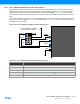
Table 38-8 shows the device equivalent internal pin capacitance.
XOUT
Internal
C
EL1
C
L1
C
L2
C
P1
C
P2
C
EL2
External
XIN
C
tot
∑
C
L1
C
P1
C
EL1
++ ) C
L2
C
P2
C
EL2
++ )((
C
L1
C
P1
C
EL1
C
L2
C
P2
C
EL2
++ +++
--------------------------------------------------------------------------------------------------------
=
C
tot
∑
C
L
2
-------
=