
Data Sheet
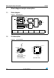
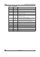

LIS3DH Block diagram and pin description
Doc ID 17530 Rev 1 9/42
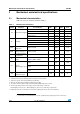
Table 2. Pin description
Pin# Name Function
1 Vdd_IO Power supply for I/O pins
2 NC Not connected
3 NC Not connected
4
SCL
SPC
I
2
C serial clock (SCL)
SPI serial port clock (SPC)
5 GND 0V supply
6
SDA
SDI
SDO
I
2
C serial data (SDA)
SPI serial data input (SDI)
3-wire interface serial data output (SDO)
7
SDO
SA0
SPI serial data output (SDO)
I
2
C less significant bit of the device address (SA0)
8CS
SPI enable
I
2
C/SPI mode selection (1: I
2
C mode; 0: SPI enabled)
9 INT2 Inertial interrupt 2
10 RES Connect to GND
11 INT1 Inertial interrupt 1
12 GND 0 V supply
13 ADC3 Analog to digital converter input 3
14 Vdd Power supply
15 ADC2 Analog to digital converter input 2
16 ADC1 Analog to digital converter input 1