
Data Sheet

Mechanical and electrical specifications LIS3DH
12/42 Doc ID 17530 Rev 1
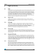
2.4 Communication interface characteristics
2.4.1 SPI - serial peripheral interface
Subject to general operating conditions for Vdd and Top.
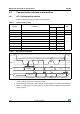
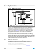
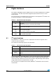
Figure 3. SPI slave timing diagram
Note: 1 Values are guaranteed at 10 MHz clock frequency for SPI with both 4 and 3 wires, based on
characterization results, not tested in production.
2 Measurement points are done at 0.2·Vdd_IO and 0.8·Vdd_IO, for both Input and output port.
3 When no communication is on-going, data on CS, SPC, SDI and SDO are driven by internal
pull-up resistors.
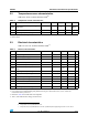
Table 6. SPI slave timing values
Symbol Parameter
Value
(1)
Unit
Min Max
tc(SPC) SPI clock cycle 100 ns
fc(SPC) SPI clock frequency 10 MHz
tsu(CS) CS setup time 6
ns
th(CS) CS hold time 8
tsu(SI) SDI input setup time 5
th(SI) SDI input hold time 15
tv(SO) SDO valid output time 50
th(SO) SDO output hold time 9
tdis(SO) SDO output disable time 50
SPC
CS
SDI
SDO
t
su(CS)
t
v(SO)
t
h(SO)
t
h(SI)
t
su(SI)
t
h(CS)
t
dis(SO)
t
c(SPC)
MSB IN
MSB OUT
LSB OUT
LSB IN
(3)
(3)
(3)
(3)
(3)
(3)
(3)
(3)