
Data Sheet

Mechanical and electrical specifications LIS3DH
10/42 Doc ID 17530 Rev 1
2 Mechanical and electrical specifications
2.1 Mechanical characteristics
Vdd = 2.5 V, T = 25 °C unless otherwise noted
(a)
a. The product is factory calibrated at 2.5 V. The operational power supply range is from 1.71V to 3.6 V.
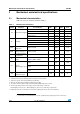
Table 3. Mechanical characteristics
Symbol Parameter Test conditions Min. Typ.
(1)
Max. Unit
FS Measurement range
(2)
FS bit set to 00 ±2.0
FS bit set to 01 ±4.0
FS bit set to 10 ±8.0
FS bit set to 11 ±16.0
g
So Sensitivity
FS bit set to 00 1 mg/digit
FS bit set to 01 2 mg/digit
FS bit set to 10 4 mg/digit
FS bit set to 11 12 mg/digit
TCSo
Sensitivity change vs
temperature
FS bit set to 00 0.01 %/°C
TyOff
Typical zero-
g level
offset accuracy
(3),(4)
FS bit set to 00 ±40 mg
TCOff
Zero-
g level change
vs temperature
Max delta from 25 °C ±0.5 m
g/°C
An
Acceleration noise
density
FS bit set to 00, Normal Mode
(Tabl e 9 ), ODR = 100Hz
220
ug/sqrt(H
z)
Vst
Self-test
output change
(5),(6),(7)
FS bit set to 00
X axis
276 LSb
FS bit set to 00
Y axis
276 LSb
FS bit set to 00
Z axis
984 LSb
Top
Operating
temperature range
-40 +85 °C
1. Typical specifications are not guaranteed.
2. Verified by wafer level test and measurement of initial offset and sensitivity.
3. Typical zero-g level offset value after MSL3 preconditioning.
4. Offset can be eliminated by enabling the built-in high pass filter.
5. The sign of “Self-test output change” is defined by CTRL_REG4 STsign bit, for all axes.
6.
Self-test output changes with the power supply. “Self-test output change” is defined as
OUTPUT[LSb]
(CTRL_REG4 ST bit=1)
- OUTPUT[LSb]
(CTRL_REG4 ST bit=0)
. 1LSb=1mg, ±2 g Full-scale.
7. Output data reach 99% of final value after 1 ms when enabling self-test mode, due to device filtering.