
User guide


DDR3 SODIMM
Product Datasheet
Rev. 1.5a Nov. 2012
11
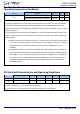
Single-Ended AC and DC Input Levels for Command and Address
DDR3-1066 DDR3-1333 Note
Symbol Parameter
Min. Max. Min. Max.
Units
VIH.CA(DC) DC Input Logic High Vref + 0.100 VDD Vref + 0.100 VDD V 1
VIL.CA(DC) DC Input Logic Low VSS Vref - 0.100 VSS Vref - 0.100 V 1
VIH.CA(AC) AC Input Logic High Vref + 0.175 Note 2 Vref + 0.175 Note 2 V 1, 2
VIL.CA(AC) AC Input Logic Low Note 2 Vref - 0.175 Note 2 Vref - 0.175 V 1, 2
VIH.CA(AC150) AC Input Logic High - - Vref + 0.15 Note 2 V 1, 2
VIL.CA(AC150) AC Input Logic Low - - Note 2 Vref - 0.15 V 1, 2
VRefCA(DC)
Reference Voltage
for ADD, CMD Inputs
0.49 x VDD 0.51 x VDD 0.49 x VDD 0.51 x VDD V 3, 4
Note:
1. For input only pins except . Vref = VrefCA(DC).
2. See “Overshoot and Undershoot Specifications” in the device datasheet.
3. The ac peak noise on VRef may not allow VRef to deviate from VRefDQ(DC) by more than +/-1% VDD (for reference:
approx. +/- 15 mV).
4. For reference: approx. VDD/2 +/- 15 mV.
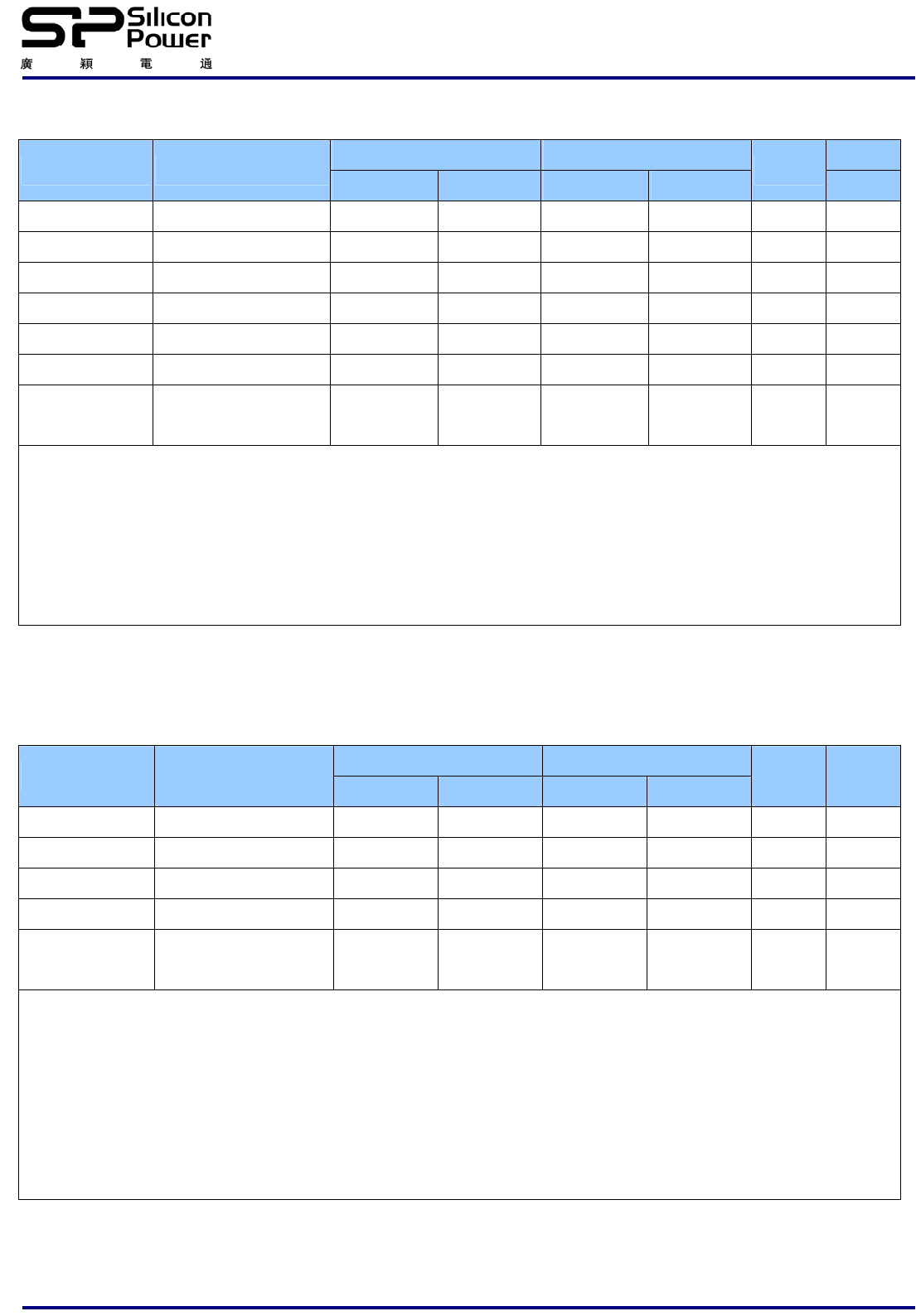
Single-Ended AC and DC Input Levels for DQ and DM
DDR3-1066 DDR3-1333
Symbol Parameter
Min. Max. Min. Max.
Units Note
VIH.DQ(DC) DC Input Logic High Vref + 0.100 VDD Vref + 0.100 VDD V 1
VIL.DQ(DC) DC Input Logic Low VSS Vref - 0.100 VSS Vref - 0.100 V 1
VIH.DQ(AC) AC Input Logic High Vref + 0.175 Note 2 Vref + 0.15 Note 2 V 1, 2, 5
VIL.DQ(AC) AC Input Logic Low Note 2 Vref - 0.175 Note 2 Vref - 0.15 V 1, 2, 5
VRefDQ(DC)
Reference Voltage
for DQ, DM Inputs
0.49 x VDD 0.51 x VDD 0.49 x VDD 0.51 x VDD V 3, 4
Note: 1. For input only pins except. Vref = VrefDQ(DC).
2. See “Overshoot and Undershoot Specifications” in the device datasheet.
3. The ac peak noise on VRef may not allow VRef to deviate from VRefDQ(DC) by more than +/-1% VDD (for reference:
approx. +/- 15 mV).
4. For reference: approx. VDD/2 +/- 15 mV.
5. Single-ended swing requirement for DQS, DQS# is 350 mV (peak to peak). Differential swing requirement for DQS -
DQS# is 700 mV(peak to peak).