DM15/25 Integrator’s Manual DM-15/25 Integrator’s Manual 1 OF 38
DM15/25 Integrator’s Manual 2 OF 38 DM-15/25 .............................................................................................................................................................................. 1 INTEGRATOR’S MANUAL............................................................................................................................................... 1 1 INTRODUCTION TO THE INTEGRATOR’S MANUAL.................................................................................
DM15/25 Integrator’s Manual 3 OF 38 6.3 PCM ..................................................................................................................................................................... 26 6.4 ANALOG AUDIO ..................................................................................................................................................... 27 6.4.1 Creating an analog ground................................................................................................
DM15/25 Integrator’s Manual 1 4 OF 38 Introduction to the Integrator’s Manual 1.1 Overview This manual is for use as a guide to the setup, installation, and use of the DM-15/25 module into your application. The module may be tested using the Developer’s Kit which is supplied together with the a DM-15/25 module and all the necessary tools. The DM-15/25 module is intended for mounting into an application developer’s chassis to provide wireless communication capability for the product.
DM15/25 Integrator’s Manual 1.
DM15/25 Integrator’s Manual 2 6 OF 38 Safety & FCC Requirements 2.1 Warning: FCC RF Exposure Requirements This module is approved for mobile operations only with respect to CFR 47 part 2.1091. If this module is intended to be used as a portable device, the OEM integrators should investigate separate approval to satisfy SAR requirements of 2.1093. 2.2 Warning: Antenna Installation • At no time is the antenna to be located closer than 27 centimeters to a normally occupied location or person.
DM15/25 Integrator’s Manual 7 OF 38 2.8 Potentially Explosive Atmospheres Turn your module off when in any area with a potentially explosive atmosphere and obey all signs and instructions. Sparks in such areas could cause an explosion or fire resulting in bodily injury or even death. Areas with a potentially explosive atmosphere are often, but not always, clearly marked.
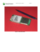
DM15/25 Integrator’s Manual Figure 1: DM-15/25 Module 8 OF 38
DM15/25 Integrator’s Manual 4 9 OF 38 Integrating The DM-15/25 Module 4.1 Mechanical Description The DM-15/25 has no mechanical elements other than the main PCB assembly. All critical electronic components are shielded using sheet metal cans to prevent internal and external electromagnetic interference from degrading the module’s performance and to prevent the module from interfering with other nearby devices.
DM15/25 Integrator’s Manual 10 OF 38 The following shows the allowed contact area to the module. Contact to areas other than the areas shown below should be avoided due to the possibility that electrical components or pc-board connectors may be exposed. Note also a “Heat Sink”area is shown. This contact point can be used for contacting a heat sink if needed when operation within the user’s enclosure restricts air flow. Figure 4 Contact Areas for the DM-15/25 4.1.
DM15/25 Integrator’s Manual Figure 2: 30-pin system connector 11 OF 38
DM15/25 Integrator’s Manual 12 OF 38 Figure 3: 30-pin system connector footprint Section 4.1.3.2 shows the PIN-connection of the different signals connected to the interface as well as a short description of the signals.
DM15/25 Integrator’s Manual 4.1.2 13 OF 38 General Electrical and Logical Characteristics Many of the signals present in the interface are CMOS signals where the following levels apply. CMOS Output / Input electrical characteristics Parameters Test conditions Limits Units Min. 4.1.3 Typ. Max. High level output voltage (IOH= 800 µA) VOH 0.9 * VDD VDD Low level output voltage (IOL= 800 µA) VOL 0 0.1* VDD Volts High-Level Input Voltage (VIH) VIH 0.
DM15/25 Integrator’s Manual 14 OF 38 4.1.3.1 Power Consumption 4.1.3.1.1 Transmit Mode Power class selection VCC_5V (peak) VCC_12V (peak) Heat Sink Busrt Mode Class I AMPS Class II TDMA Class II 600-ma 1,300-ma 9o C/watt recommended Busrt Mode Class I AMPS Class IV TDMA Class IV 1,000-ma 1,300-ma Not required Table 2 Power Consumption in Transmit/talk mode 4.1.3.1.2 Standby Mode DC current in mA Average AMPS Mode 45 TDMA Mode 45 PCS Mode 35 Table 3 Power Consumption in Standby Mode 4.1.
DM15/25 Integrator’s Manual 15 OF 38 MODEL Description DM15 800 MHz, Class 4 TDMA/AMPS, Single 5-V supply +/-10% DM-15A, 800 MHz, Class 4 TDMA/AMPS; Class 1 Burst Data; Dual Supply required (+5v +/-10%, 13.8v +/- 20%) Selectable mode for Class 2 TDMA/AMPS; Class 1 Burst Data , Dual Supply required (+5v +/-10%, 12v +/- 10%) DM-25 800/1900 MHz, Class 4 TDMA/AMPS, Class 1 Burst Data, Dual Supply required (+5v +/-10%, 13.
DM15/25 Integrator’s Manual 16 OF 38 Chassis Ground (GND) GND is the logical reference of all digital signals in the System Interface as well as the DC return of the power supply signal, VCC_5V and VCC_12V (used for AMPS burst modes). Electrical characteristics: Iaverage < 0.7 A Ipeak < 2 A Note! That no GND pin can withstand over 0.5 A. 4.1.3.3 MODULE_PWR_EN_B (WAKE) The MODULE_PWR_EN_B (WAKE) signal is a TTL compatible active high input.
DM15/25 Integrator’s Manual 17 OF 38 Pin DM-15/DM-25 Description 3 AFMS Audio Output From Module 6 ATMS Audio Input to Module The factory default audio settings are presented in the following table. Refer to AT*NAUD AFMS Module audio output Output Impedance (active state) Output Impedance (inactive state) Output Impedance (pwr down state) Drive capacity into 50 Ω Drive capacity into 5 kΩ External Device audio input Input Impedance Volume control ATMS (0.3 – 3.
DM15/25 Integrator’s Manual 18 OF 38 Pin DM-15/DM-25 Description 13 PCMCLK External PCM Clock Output 14 PCMSYNC External PCM frame Sync 15 PCMULD External PCM Voice Input 16 PCMDLD External PCM Voice Input Already defined CMOS output/input electrical characteristics apply (see Section 4.1.2 General Electrical and Logical Characteristics). The voltage levels at the PCM interface are in accordance with the 3.3 V DC CMOS technology.
DM15/25 Integrator’s Manual 19 OF 38 4.1.4.2.2 Timing Timing shall be according to the following diagram (see Figure 4). The signals in the diagram shall be interpreted according to the following relation. DM-15/DM-25 signal Diagram name PCMCLK PCMCLK (output) PCMSYNC PCMSYN (output) PCMULD PCMI (input) PCMDLD PCMO (output) Figure 4 PCM timing diagram for DM-15/DM-25 The meaning and value of the timing parameters are described in Table 4.
DM15/25 Integrator’s Manual 4.1.5 20 OF 38 Serial Data Interface The serial channels are used as asynchronous communication links between the application system and the module.
DM15/25 Integrator’s Manual Pin DM-15/DM-25 Description 7 OUTPUT 2 General Purpose Binary Output # 2 9 INPUT 2 General Purpose Binary Input # 2 10 OUTPUT 1 General Purpose Binary Output # 1 12 INPUT 1 General Purpose Binary Input # 1 21 OF 38 The general purpose output signals OUTPUT 1 and OUTPUT 2 are CMOS open drain outputs with 1 mA drive. The general purpose input signals INPUT 1 and INPUT 2 are CMOS bi-directional, tri-state output with 2mA drive. 5 Application IO description 5.
DM15/25 Integrator’s Manual 22 OF 38 The pin direction in this table is seen from the application’s point of view. Group Pin No. Name Application Requirements App I/O1 HW flow control is by default enabled in the phone module. 23 TD (DTMS) 26 RD (DFMS) 24 RTS 21 CTS 22 DTR 19 VPPFLASH/DCD Data Data Logic output to phone module. The application shall set this output active high upon startup. Logic input from phone module. Logic output to phone module.
DM15/25 Integrator’s Manual 5 Analog Audio 6 3 8 23 OF 38 Analog reference. This signal is an analog reference output by the phone module. This signal is connected to GND in one place in the phone module. Under no AGND circumstances shall it be connected to any ground or be used as ground in the application. See 3.4 for more detailed information. ATMS Single ended audio output to phone module. AFMS Single ended audio input from phone module.
DM15/25 Integrator’s Manual 6 24 OF 38 Recommended Circuitry Abbreviations: • VCC • VREF Represents the logic supply voltage used by the application. Represents the logic supply voltage used by the phone module. Component proposals: • Transistors not showing a base resistor should be interpreted as a BRT (Built in Resistor Transistor) i.e. Toshiba RN1308. • The inverting buffers should preferably be Schmitt-Triggered, i.e. Toshiba TC7S14 or similar. 6.
DM15/25 Integrator’s Manual 25 OF 38 6.1.1 MODULE_PWR_EN_B (Wake) This signal, located on pin 12 in the system connector, enables the main 5V supply in the phone module so that it powers on. This is an open collector input to the phone module. Its reference voltage is the main 5V supply. 6.2 Data The data group contains six signals, three output signals from application, two input signals to application, and one I/O signal.
DM15/25 Integrator’s Manual 6.2.1 26 OF 38 VPPFLASH/DCD This signal, located on pin 23 in the system connector, can be used by the application to enable flashing of the phone module. To enter flash-mode, the application shall set VPPFLASH_EN active high, then enable the MODULE_PWR_EN_B pin. The circuitry above ensures that a high enough signal is input on VPPFLASH without overloading the DCD input buffer. 6.
DM15/25 Integrator’s Manual 6.4 27 OF 38 Analog Audio 6.4.1 Creating an analog ground An analog ground plane should be generated, which connects to GND in one point so that high frequency digital current is not floating through the analog ground. Connecting the analog ground in only one point avoids ground currents from power supplies and other high current circuitry from creating noise in the analog circuitry.
DM15/25 Integrator’s Manual 28 OF 38 6.4.2 Creating an analog reference voltage (BIAS) The BIAS reference should be generated from the analog supply voltage (VANA) and be referenced to the analog ground. This reference shall be used to bias all analog circuitry in the application. VANA 100k - 0 BIAS + 100k The bias can be tapped directly from the resistor voltage divider, but the amplifier will make the bias more stable and less susceptible to noise.
DM15/25 Integrator’s Manual 6.4.3 29 OF 38 Analog ground vs. AGND The AGND signal output from the module is not a ground. It is an analog reference, which is connected to the main ground used by the module in one place inside the module. It should not under any circumstances be used as a ground or connected to a ground in the application. AGND must be treated as a signal. Together with ATMS and AFMS it creates a semi differential interface.
DM15/25 Integrator’s Manual 6.4.5 30 OF 38 Loudspeaker path An application using the analog audio interface must re-reference the AFMS-signal from AGND to its own internal BIAS. The figure shows a differential implementation. C1 is chosen to create the correct HP frequency response. R1 and R2 determine the gain, and C2 and R2 determine the LP frequency response. C2 R2 AFMS C1 R1 >=10k 0 - Internal App + 0 AGND + C1 R1 >=10k Internal App R2 C2 BIAS 6.4.
DM15/25 Integrator’s Manual 31 OF 38 Electrical characteristics at the antenna interface Nominal impedance 50 Ω (better than 2:1) Output Power 3 Watt peak (Class 1) Burst Modem, AMPS 2 Watt peak (Class 2) AMPS, DAMPS 0.6 Watt peak (Class 4) AMPS, DAMPS, PCS Better than - 116 dBm 12 dB SINAD, AMPS Better than - 110 dBm <3% BER, DAMPS Better than –110 dBm <3% BER, PCS Static Sensitivity 6.5 Functional Description This chapter describes the functionality of the DM-15/DM-25 module.
DM15/25 Integrator’s Manual 32 OF 38 • Conference Calls (Multiparty). Permits the module to maintain simultaneous communication with more than one party. • Call Barring. Allows the module to bar certain categories of outgoing or incoming calls. The categories are determined by one or more barring programs. Note! Some value carrier services as Call Forwarding and Call Waiting may vary depending on your service provider’s network.
DM15/25 Integrator’s Manual 6.5.4 33 OF 38 Data Functionality 6.5.4.1 TDMA • Asynchronous Circuit Switch Data (CSD) according to EIA/TIA 136-350. AMPS • AMPS Data over the voice channel. In this case an external modem connected to the analog audio signals (ATMS, AFMS) is needed. • Microburst/Vburst mode (by Aeris). • The DM-15/DM-25 module supports Aeris Microburst and Vburst protocols. These protocols enable applications to send either short messages or 1045 byte data-grams to the Aeris data center.
DM15/25 Integrator’s Manual 34 OF 38 Burst modem application -Natural Microsystems AG/4000 Card. - Four T1 Lines, 96 ports. T1 Host Modem Server BS Automatic Call Director T1 module V.27ter modem RX/TX data PBX control (Digital PBX) T1 MSC operator T1 data base Application Server PSTN The 250 Byte Message Protocol The key feature of the 250-byte protocol is that it allows applications to send up to 250 bytes of data during a voice call.
DM15/25 Integrator’s Manual 35 OF 38 mode. This means that applications that want to use both modes may choose a different carrier for NAM-2. Using different carriers raises some complications with IRDB settings. . 6.5.6 Over the air activation (OTA) The DM-15/DM-25 supports Over the Air Programming as defined in EIA/TIA 136 Rev. B 6.5.
DM15/25 Integrator’s Manual 36 OF 38 6.5.10 Network and subscription Make sure that the AMPS/TDMA network provides the necessary telecommunication services. Contact your service provider. Make sure that the location at which you intend to use the module is within the network coverage. If you intend to use SMS for the application, make sure that this is included in your (voice) subscription. 6.5.10.1 Possible communication disturbances • Noise can be caused by electronic devices and radio transmitters.
DM15/25 Integrator’s Manual 7 37 OF 38 Technical Data Mechanical specifications Maximum length: 4.050 in Maximum width: 1.827 in Maximum thickness: 0.50 in Weight: 44 g Power supply voltage, normal operation VCC_5V VCC_12V Nominal Voltage: 5.00 Volts 13.8 Volts Class I 12.0 Voltts Class II Voltage range: 4.5 – 5.5 Volts 11.1 – 16.6 Volts Class I 10.8 – 13.2 Volts Class II Power Consumption (Maximum): 1 Amps (1A Peak during TDMA Burst) 1.
DM15/25 Integrator’s Manual 38 OF 38 Stationary vibration, random Acceleration spectral density (m2/s2): 0.96 2.88 0.96 Frequency range: 5-10 10-200 200-500 60 min per/axis Non-stationary vibration, including shock Shock response spectrum I, peak acceleration: - 3 shocks in each axis and direction: 300 m/s2, 11 ms Shock response spectrum II, peak acceleration: - 3 shocks in each axis and direction: 1000 m/s2, 6 ms Bump: Acceleration 250 m/s2 Free fall transportation: 1.